System and methods for classifying anomalies of sample surfaces

a sample surface and anomaly technology, applied in the field of sample surface anomalies detection systems, can solve the problems of different sources of defects, unique set of defects, and different impacts on the final device yield, and achieve the effect of improving yield

Inactive Publication Date: 2006-05-02
KLA CORP
View PDF10 Cites 17 Cited by
  • Summary
  • Abstract
  • Description
  • Claims
  • Application Information

AI Technical Summary

Benefits of technology

[0012]This invention is based on the observation that, by varying the sensitivity by which the anomalies are detected to provide output(s) or by varying a threshold when data on the anomalies are analyzed, more information useful for classifying the anomalies becomes available. By using outputs obtained at two or more different detection sensitivities, or by processing the data on the anomalies using two or more different thresholds, it is possible to distinguish between microscratches and particles, pits or other point defects. At least one classification of the anomalies may then be provided. Preferably, this can be done without requiring a user to scan the sample surface more than one time. This will permit a user to distinguish between microscratches from particles and other point defects and adjust the CMP or cleaning process in real time in an on-line production process or post-processing as required to improve yield.

Problems solved by technology

The combination of the chemical reaction and abrasive behavior of the CMP process creates a unique set of defects, such as microscratches, chatter marks, slurry residue, etc.
The adoption of CMP presents a great opportunity to have a better DOF budget, but poses a unique challenge in the inspection of processed CMP wafers, along with achieving higher chip yield by using appropriate yield management techniques.
In general, different types of defects have different sources and different impacts on the final device yield.
This places ever-greater demands on yield management and in particular on defect inspection and classification during the CMP process; the loss of a single production wafer leads to a significant revenue loss.
Due to the nature of the process, CMP microscratches are very difficult, if not impossible, to avoid.
Depending upon their dimensions and locations, these defects may adversely affect the yield of the device.
Intrinsic defects include such defects as microscratches, chatter marks, water marks, long scratches (continuous and spiral), pits, rip-out and dishing.
Due to the complexity of the patterned wafers, additional types of defects are present.
These defects are related to the manufacturing process.
As the name implies, residual slurry results from incomplete or improper cleaning after the CMP step.
Other factors that contribute to microscratch generation include unsuitable rinsing and buffing steps following the CMP step.
Although buffing with soft pads over hard pads reduces the formation of microscratches, incorrect buffing produces worse results.
The dilute-HF dip step, which follows the buffing polish step, can increase the number of micro-scratches, enlarges existing microscratches, and leads to failure of the device.
However, many scratches produced during the CMP processors are smaller than that and may even be smaller than the spot size of the laser beam used in the system.
Therefore, without using a classification method, the user would not be able to distinguish between microscratches from particles or other types of point anomalies such as pits on the wafer surface.
When there are a large number of defects on the wafer surface, such method is time consuming and not practical for use in a production environment.

Method used


Image

  • System and methods for classifying anomalies of sample surfaces
  • System and methods for classifying anomalies of sample surfaces
  • System and methods for classifying anomalies of sample surfaces

Examples


Embodiment Construction

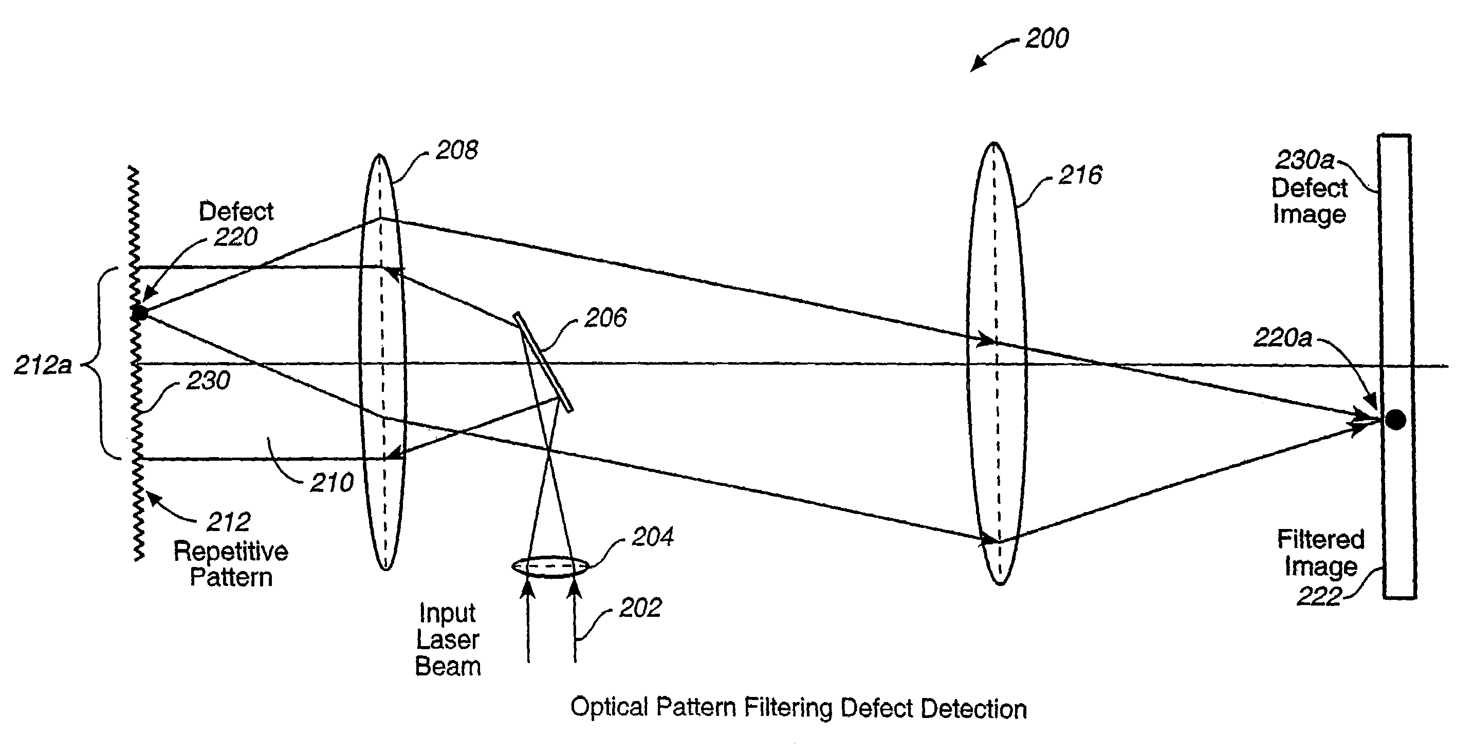
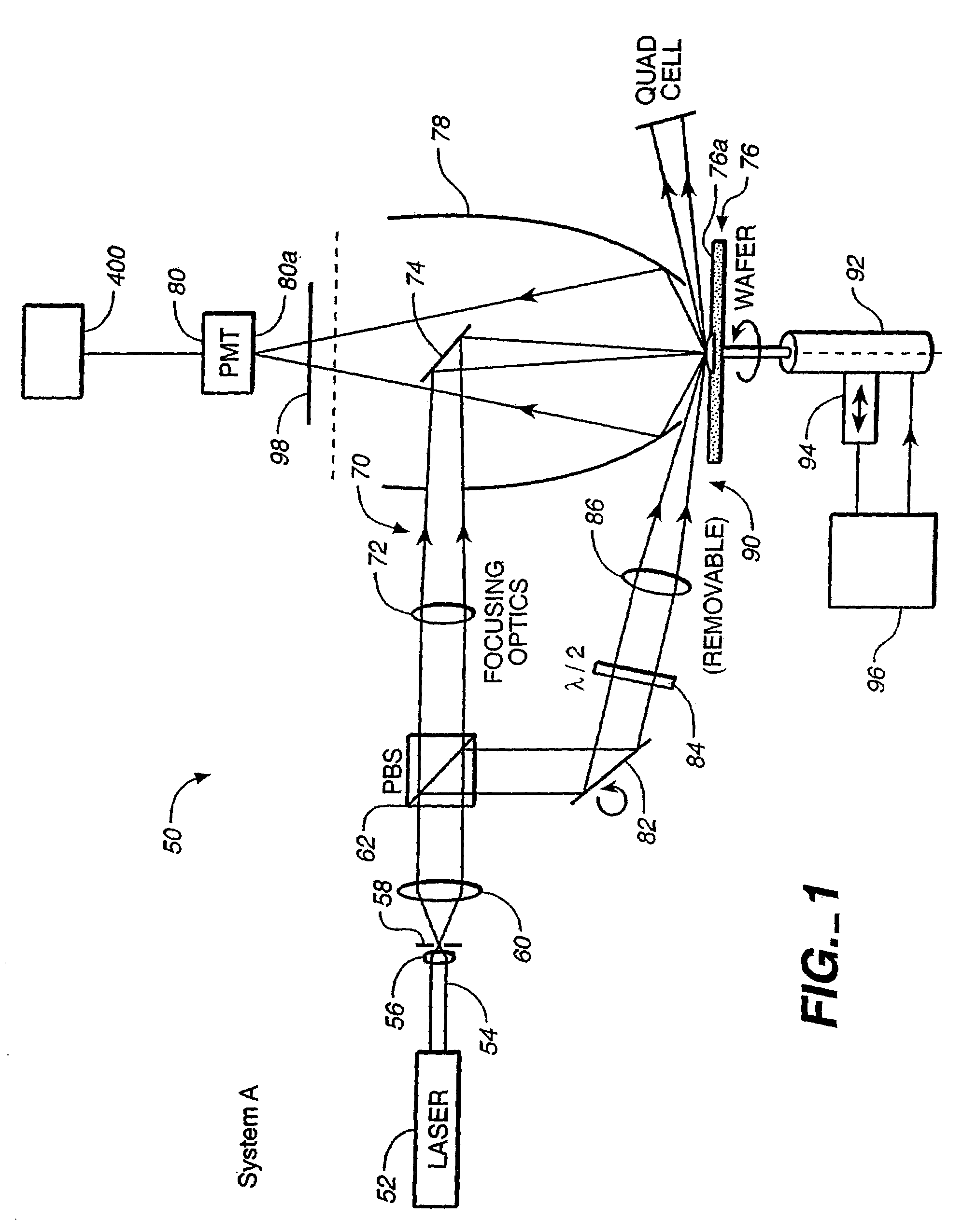
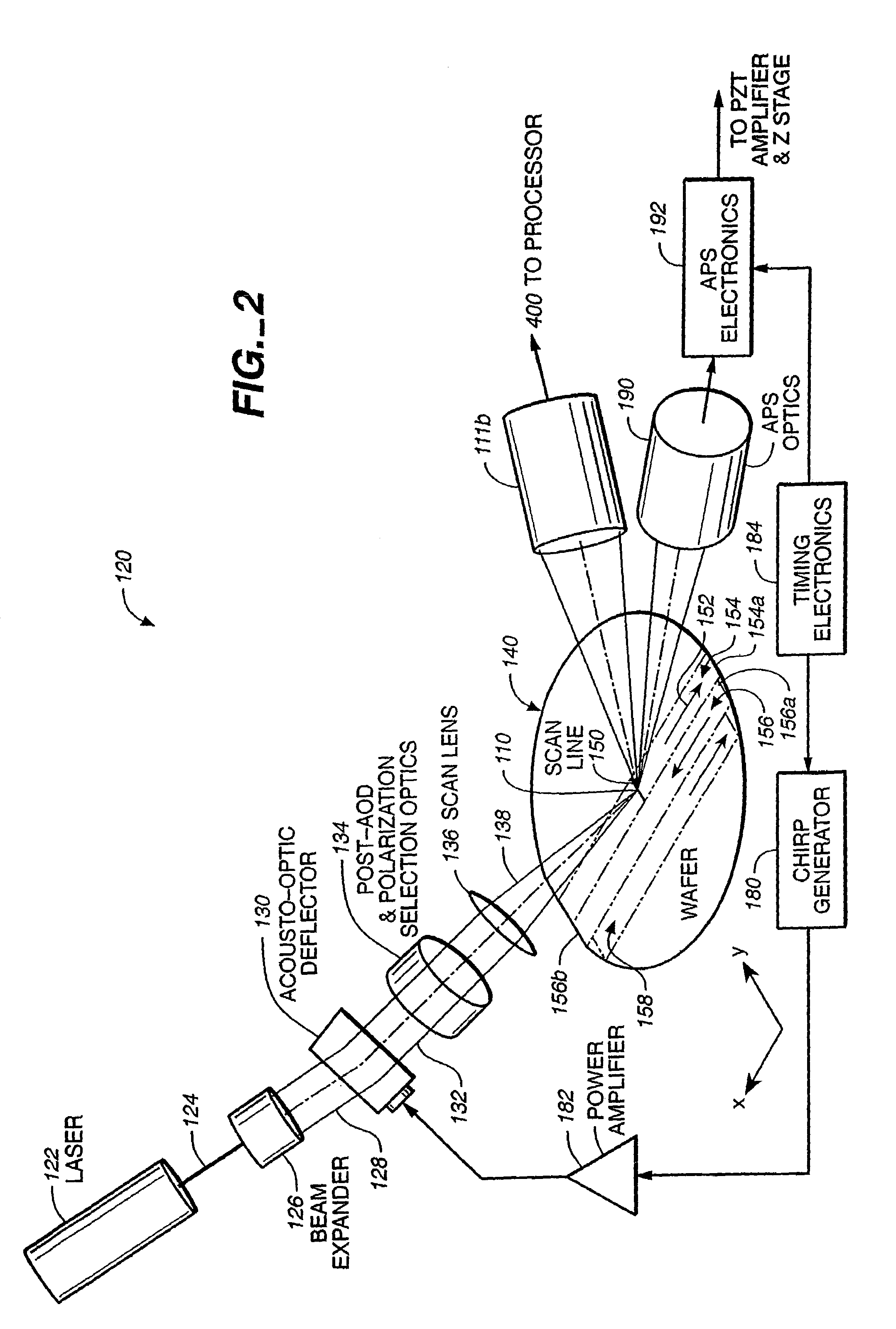
[0025]As noted above, the Surfscan SPITBI® instrument available from the assignee of the present application, KLA-Tencor Corporation, may be used for inspecting semiconductor wafer surfaces, such as those of unpatterned wafers, as well as other sample surfaces, such as those of magnetic or optical disks for storage and flat panel display type devices. A description of such system is set forth in U.S. patent application Ser. No. 08 / 933,771, filed on Sep. 19, 1997, entitled “Improved Sample Inspection System.” This application is incorporated herein by reference in its entirety, and is referred to herein as the companion application. While the description below of the Surfscan SPITBI® instrument taken from such application describes anomaly detection of semiconductor wafer and film surfaces, it will be understood that essentially the same instrument and process may be used for defect detection of other samples such as magnetic or optical disks used for information storage and flat pan...


PUM

PropertyMeasurementUnit
sizeaaaaaaaaaa
lengthaaaaaaaaaa
sizeaaaaaaaaaa

Abstract

Two or more defect maps may be provided for the same sample surface at different detection sensitivities and / or processing thresholds. The defect maps may then be compared for better characterization of the anomalies as scratches, area anomalies or point anomalies. This can be done without concealing the more significant and larger size defects amongst numerous small and immaterial defects. One or more defect maps can be used to report the anomalies with classified information; the results from this map(s) can be used to monitor the process conditions to obtain better yield.

Description

CROSS-REFERENCE TO RELATED APPLICATIONS[0001]This application is a divisional application of U.S. application Ser. No. 09 / 566,352, filed May 4, 2000, entitled “System and Methods for Classifying Anomalies of Sample Surfaces,” now U.S. Pat. No. 6,590,645.BACKGROUND OF THE INVENTION[0002]This invention relates in general to systems for analyzing anomalies of sample surfaces, such as those of semiconductors and those of magnetic or optical disks or flat panel displays, and in particular, to a system for detecting and classifying anomalies of such surfaces.[0003]Achieving the best possible financial performance drives the continuous shrinkage of the critical dimensions of integrated circuit devices that are fabricated on surfaces of semiconductor wafers. This shrinkage requires a flatter wafer surface due to limited lithographic depth of focus (DOF) and higher circuit packing density, along with many other factors. Chemical mechanical planarization or polishing (CMP) has become an enabl...

Claims


Application Information

Patent Timeline
Patent Type & Authority Patents(United States)
IPC IPC(8): G01N21/00G01N21/88G01N21/95H01L21/66
CPCG01N21/8851G01N21/9501H01L22/26G01N21/9506H01L22/12
Inventor CHEN, WAYNEZENG, ANDREWAKBULUT, MUSTAFA
Owner KLA CORP
Why Eureka
Try Eureka