Modeling custom scan flops in level sensitive scan design

a scan cell and scan design technology, applied in the field of integrated circuit design testing, can solve the problems of significant fault coverage loss, negative impact on the performance of the circuit, coverage loss, etc., and achieve the effect of simplifying the testing of the microprocessor implementing the scan cell, minimizing adverse effects on the performance of the microprocessor, and improving the percentage of faults

Inactive Publication Date: 2006-05-02
ORACLE INT CORP
View PDF15 Cites 7 Cited by
  • Summary
  • Abstract
  • Description
  • Claims
  • Application Information

AI Technical Summary

Benefits of technology

[0010]The illustrative embodiment of the invention significantly improves the percentage of faults in a circuit design that are detected in ATPG tools, such as FastScan and TetraMAX. Moreover, testing of a microprocessor implementing the scan cell is simplified, and the testing procedure minimizes adverse effects on the performance of the microprocessor.

Problems solved by technology

However, many of the currently available ATPG tools used with LSSD cause significant fault coverage loss and test coverage loss and have a negative impact on the performance of the circuit.
In other words, many potential design defects cannot be simulated and tested using these tools and of the design defects that can be simulated and tested for, many often go undetected.

Method used


Image

  • Modeling custom scan flops in level sensitive scan design
  • Modeling custom scan flops in level sensitive scan design
  • Modeling custom scan flops in level sensitive scan design

Examples


Embodiment Construction

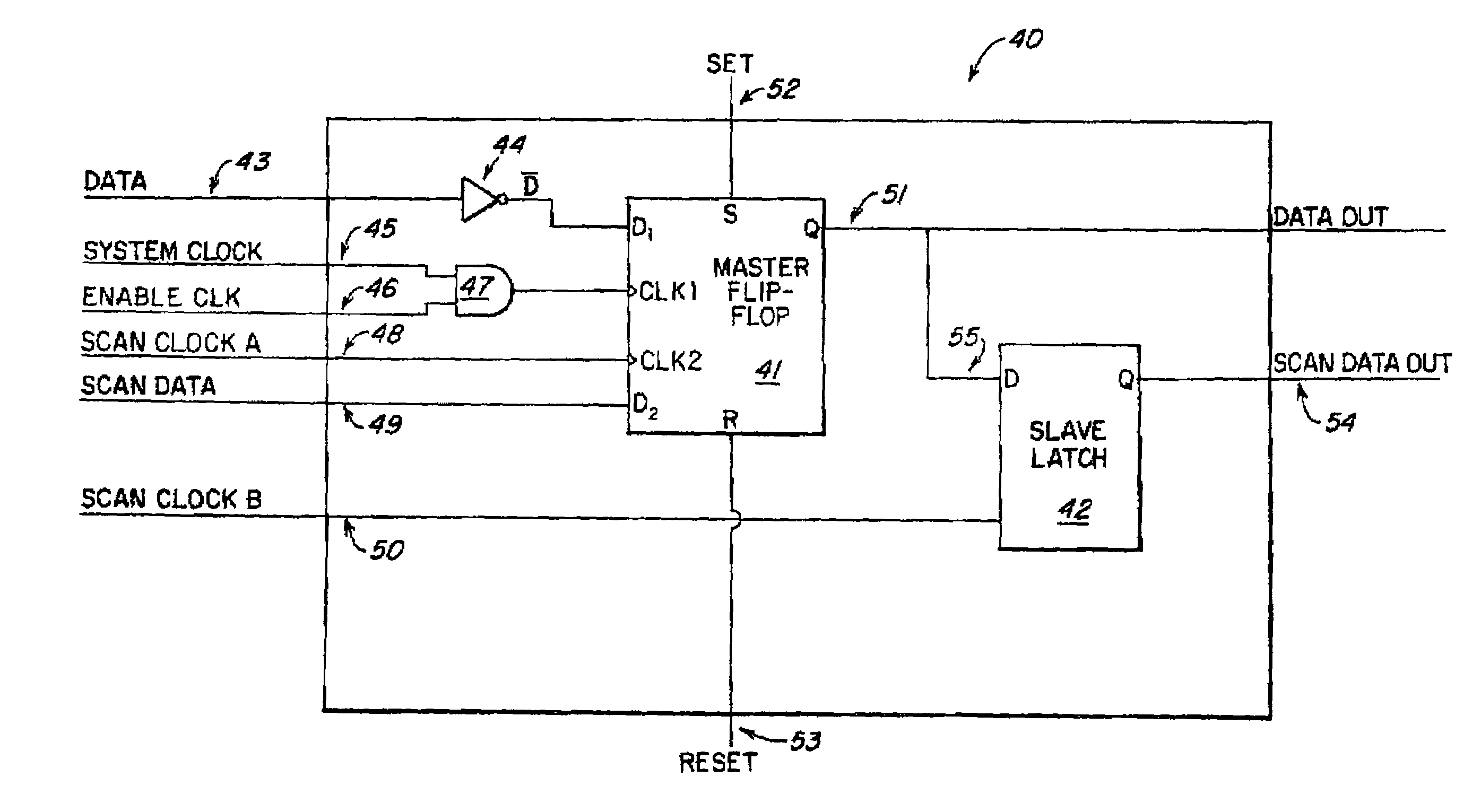
[0021]The illustrative embodiment provides an improved testing design for ATPG for detecting faults in an integrated circuit. The illustrative embodiment enables automatic testing of integrated circuit designs and provides a high fault coverage without compromising performance. The illustrative embodiment is implemented in the design and testing of UltraSparc processors, developed by Sun Microsystems. One skilled in the art will recognize that the invention is not limited to UltraSparc processors and may be utilized to design and test any suitable integrated circuit.

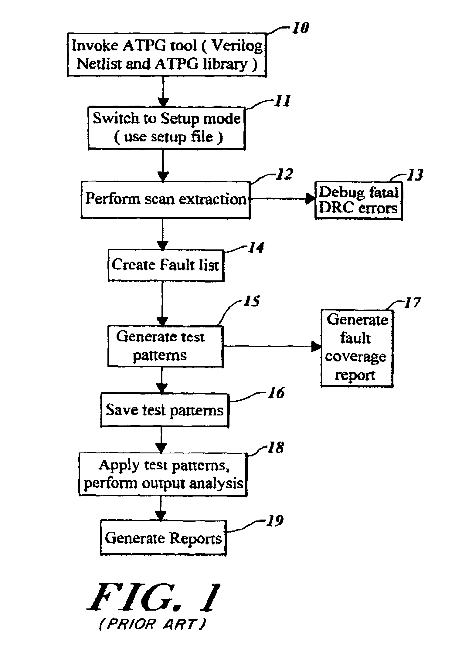
[0022]The scan cell of the illustrative embodiment of the present invention scans test patterns generated via ATPG to test a circuit design. Test data generated by the ATPG process illustrated in FIG. 1 is shifted through the scan cell of the illustrative embodiment during test mode to detect faults in the circuit design. One skilled in the art will recognize that the present invention is not limited to these ATPG tools,...


PUM


Abstract

A system and method for testing an integrated circuit is provided. The illustrative embodiment provides a scan cell for use with automatic test pattern generation (ATPG). In the scan cell of the illustrative embodiment, a flip-flop is configured as a master storage element and a latch is configured as a slave storage element. During standard operating mode, the flip-flop and the latch operate as standard storage elements in the circuit. During a test mode, the flip-flop and the latch form a shift register for shifting test pattern data through the circuit to identify and detect any faults in the circuit design.

Description

FIELD OF THE INVENTION[0001]The present invention relates to testing integrated circuit designs using automatic test pattern generation (ATPG).BACKGROUND OF THE INVENTION[0002]An important step in the development and design of an integrated circuit is testing to detect faults in the circuit design. Testing of an integrated circuit generally involves adding partial or full scan to a circuit design using an ATPG program. The ATPG program generates a set of test patterns to identify faults in the integrated circuit design, which are applied to the input pins of the integrated circuit under test. The response of the integrated circuit to the test patterns is examined at the output pins of the integrated circuit to detect logic faults in the circuit design. A test pattern generally comprises a sequence of bits in the form of a vector, which is sequentially shifted through the storage elements of the integrated circuit.[0003]FIG. 1 is a flow chart diagramming the steps involved in ATPG fo...

Claims


Application Information

Patent Timeline
Patent Type & Authority Patents(United States)
IPC IPC(8): G01R31/28G01R31/3183G01R31/3185G11C29/36
CPCG01R31/318307G11C29/36G01R31/318541G11C2029/3202
Inventor ZHANG, AITEEN
Owner ORACLE INT CORP
Why Eureka
Try Eureka