Light emitting device

a light-emitting device and light-emitting technology, applied in the field of light-emitting devices, can solve the problems of low reliability, heat-resistance stability, durability, and inability to change the counter potential pixel by pixel or line, and achieve the effect of improving the accuracy of light-emitting devices and reducing the cost of light-emitting devices

Inactive Publication Date: 2006-05-09
SEMICON ENERGY LAB CO LTD
View PDF25 Cites 45 Cited by
  • Summary
  • Abstract
  • Description
  • Claims
  • Application Information

AI Technical Summary

Benefits of technology

[0019]Also, the invention provides a light-emitting device which is made not dependent upon transistor characteristic by controlling the amount of a current flowing through the light-emitting element. More specifically, a current source is arranged within the pixel, to supply a signal current supplied from the current source to the light-emitting element. This makes it possible to supply a constant value of signal current to the light-emitting element freely from the characteristic variation between the transistors configuring the pixel.
[0040]Meanwhile, in the case that the light-emitting-device driving scheme adopts a time-gray-scale scheme, a reverse bias is applied during a period the light-emitting element is out of light emission thereby making it possible to apply a reverse bias without affecting gray scale representation.

Problems solved by technology

However, the light-emitting element is not resistive to the moisture or oxygen in air, thus involving a problem of low reliability, heat-resisting stability, durability and the like due to the deterioration in an organic compound layer.
However, the counter potential of a light emitting element, in many cases, is connected to a line common to all the pixels, making it impossible to change the counter potential pixel by pixel or line by line.
Thus, there is a difficulty in changing the timing of the counter potential.
However, the polysilicon transistor formed of polysilicon involves a problem that its electrical characteristic readily varies due to the defects in grain boundaries.
Furthermore, there occurs unevenness in the emission-light brightness on the pixels of the screen, resulting in blurs.

Method used


Image

  • Light emitting device
  • Light emitting device
  • Light emitting device

Examples


embodiment 1

[Embodiment 1]

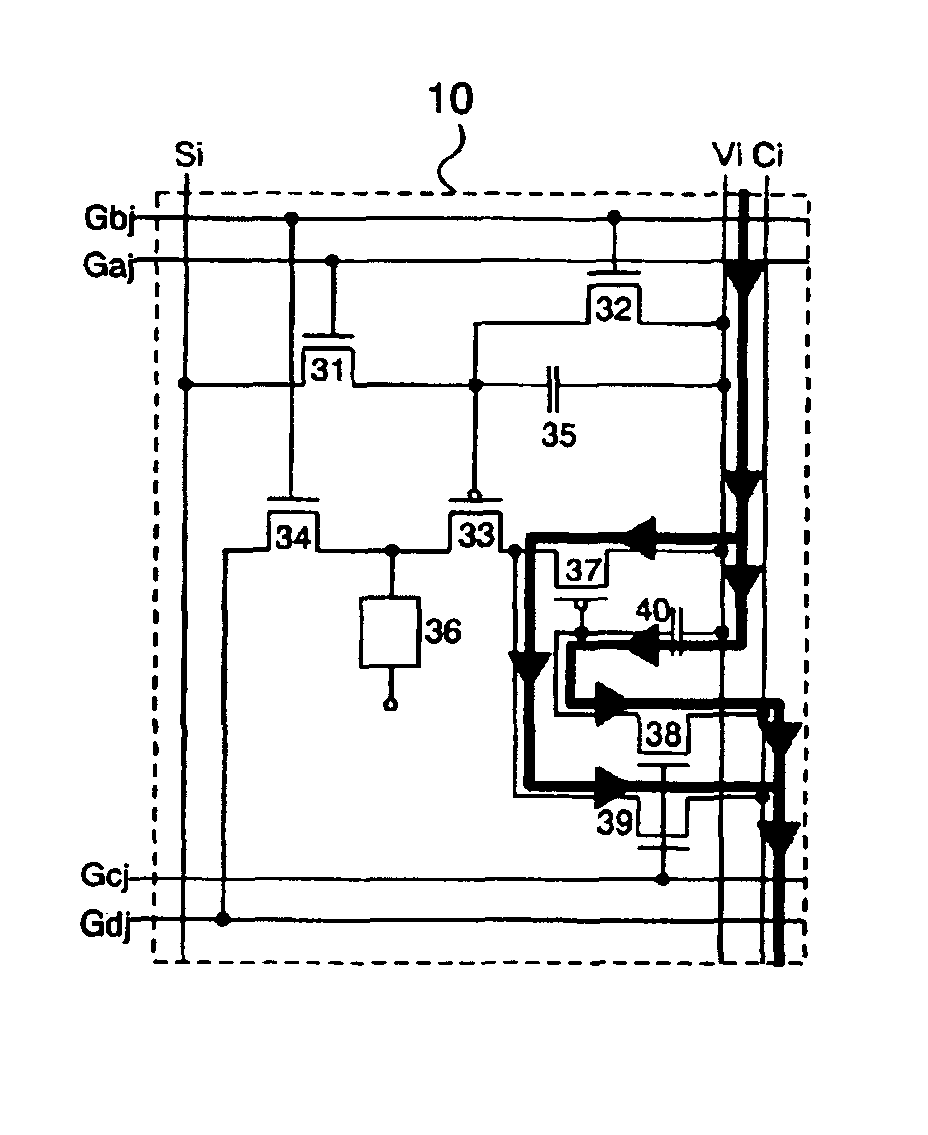
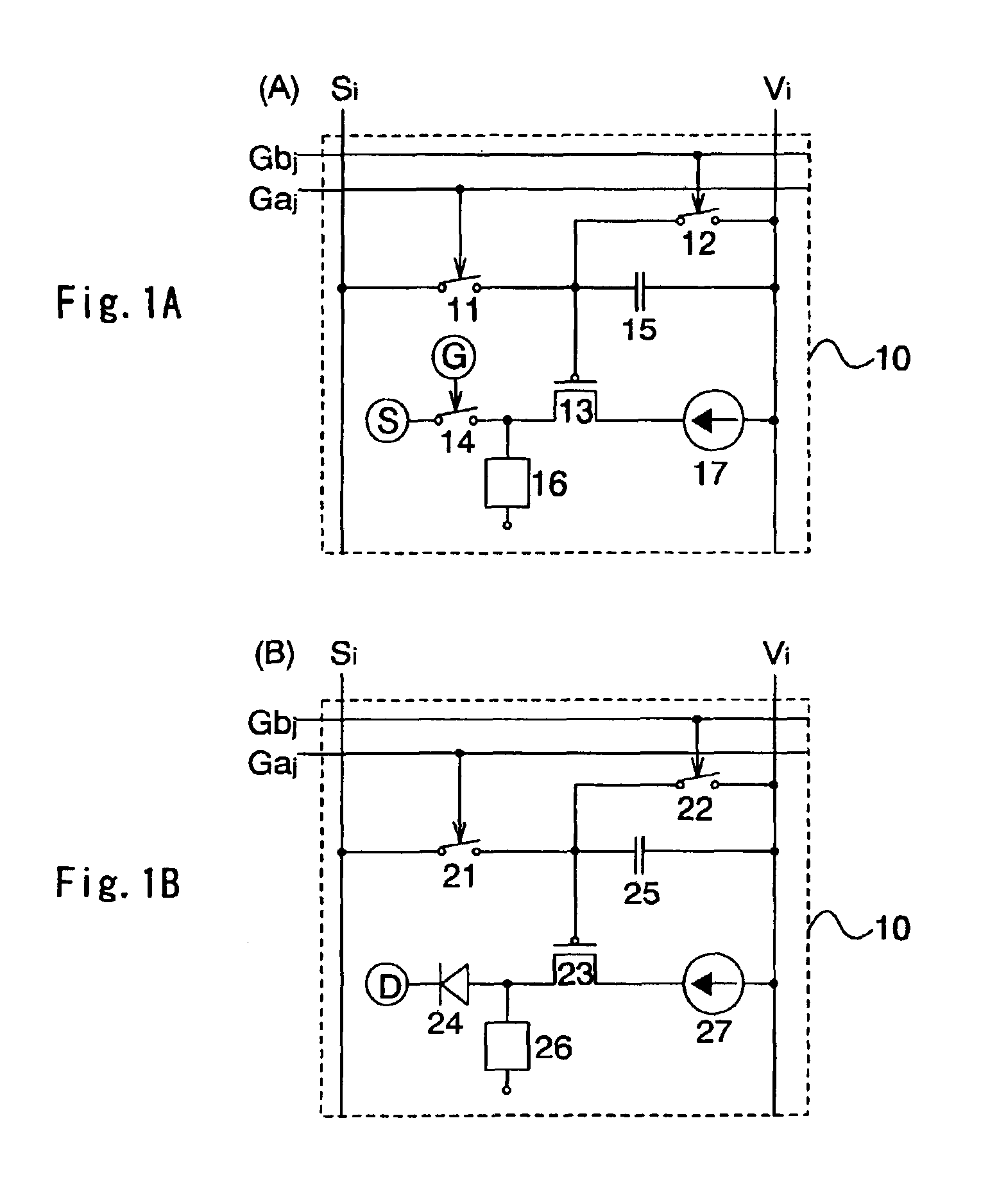
[0062]Although the pixel of the light-emitting device of the present invention was outlined two kinds by using FIGS. 1A and 1B, this embodiment explains a detailed configuration example and operation of the pixel of FIG. 1A by using FIGS. 2A to 2C, 4A and 4B. Specifically, explanation is made on a case that devising is made for a connection of the gate electrode of the discharge transistor 14 configuring for the pixel 10 shown in FIG. 1A, by using FIGS. 2A to 2C, 4A and 4B. Furthermore, explanation is made on a layout of the pixel 10 shown in FIGS. 2A to 2C, by using FIGS. 3A and 3B.

[0063]In FIG. 2A, the pixel 10 includes a select transistor 31, an erase transistor 32, a drive transistor 33, a discharge transistor 34, a capacitance element 35, a light-emitting element 36, a current-source transistor 37, a set transistor 38, a set transistor 39 and a capacitance element 40. Also, the pixel 10 has a first scanning line (Gaj)—a fourth scanning line (Gdj), a signal line (S...

embodiment 2

[Embodiment 2]

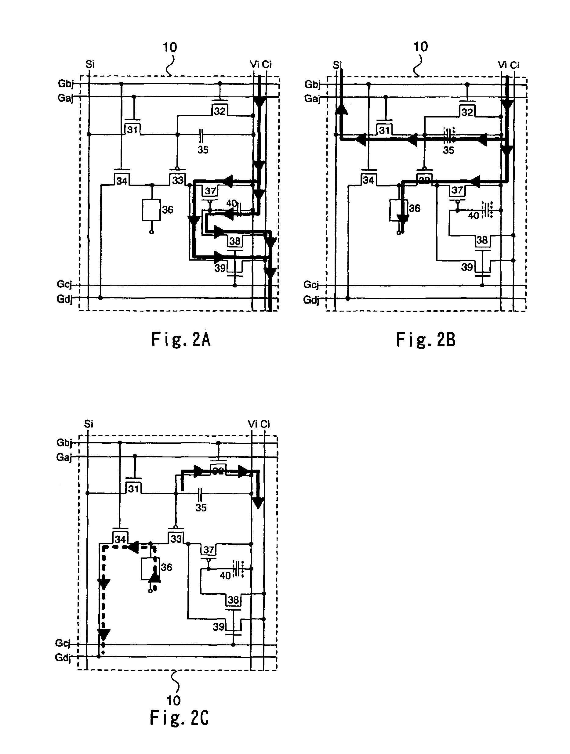
[0087]Embodiment 1 explained the case that devising is made for the connection of the gate electrode of the discharge transistor 14 of FIG. 1A. This embodiment explains a case that devising is made for a connection of the source electrode of the discharge transistor 14 of FIG. 1A using FIGS. 5A to 5D.

[0088]The pixel 10 shown in FIG. 2A and the pixel 10 shown in FIGS. 5A to 5D are the same in the number of the elements configuring the pixel 10 and the connection relationship between the elements excepting the difference in connection of the discharge transistor 34 (hereinafter, denoted as a transistor 34), and hence detailed explanation is omitted in this embodiment.

[0089]In FIGS. 5A to 5D, the transistor 34 has a gate electrode connected to the fourth scanning line (Gdj). In the pixel 10 shown in FIG. 5A, the transistor 34 has a source electrode connected to the first scanning line (Gaj) while, in the pixel 10 shown in FIG. 5B, the transistor 34 has a source electrode ...

embodiment 3

[Embodiment 3]

[0095]Although two kinds or more of the pixel outline of the light-emitting device of the invention was mentioned using by FIGS. 1A and 1B, this embodiment explains a detailed configuration example and operation of the pixel of FIG. 1B by using FIGS. 6A to 6C. Note that FIGS. 6A to 6C show, as a discharge diode 24, a transistor in diode connection.

[0096]The pixel 10 shown in FIG. 2A and the pixel 10 shown in FIGS. 6A to 6C are the same in the number of the elements configuring the pixel 10 and the connection relationship between the elements except the difference in connection of the discharge transistor 34 (hereinafter, denoted as a transistor 34), and hence the details on the connection of elements are omitted in this embodiment.

[0097]In the pixel 10 shown in FIG. 6A, the transistor 34 is an n-channel type. The transistor 34 has a gate electrode and a drain electrode that are connected with each other. Also, the transistor 34 has a source electrode connected to the f...


PUM


Abstract

The light-emitting element has a problem that reliability, heat-resisting stability and durability are low because of the deterioration in an organic compound layer. The TFT for driving the light-emitting element has a problem that variation readily occurs in its electrical characteristic due to the defects existing in grain boundaries. The present invention provides a light-emitting device by using the fact that, by applying to the light-emitting element a drive voltage having a polarity reverse to that in light emission during each constant period, the light-emitting element is improved in current-voltage characteristic. Furthermore, the present invention provides a light-emitting device made not dependent upon transistor characteristic, by controlling the amount of a current flowing through the light-emitting element.

Description

BACKGROUND OF THE INVENTION[0001]1. Field of the Invention[0002]The present invention relates to a technique of a light emitting device, more specifically, the invention relates to a light emitting device and a driving method therefor.[0003]2. Description of the Related Art[0004]Recently, display devices for performing image display are being developed. Liquid crystal display devices that perform image display by using a liquid crystal element are widely used as display panels for mobile phones and display devices for personal computers because of advantages of high image quality, thinness, lightweight, and the like.[0005]In addition, light emitting devices using self-light emitting elements as light emitting elements are recently being developed. The light emitting device has characteristics of, in addition to advantages of existing liquid crystal display devices, for example, a high response speed suitable for dynamic image display, a low voltage, and low power consumption. Theref...

Claims


Application Information

Patent Timeline
Patent Type & Authority Patents(United States)
IPC IPC(8): G09G3/10G06F3/147G09G3/20G09G3/32G09G3/36G09G5/395
CPCG09G3/3233G09G3/3275G09G3/2011G06F3/147G09G2330/028G09G3/2022G09G5/395G09G2300/0426G09G2300/0809G09G2300/0823G09G2300/0842G09G2300/0852G09G2300/0861G09G2300/0866G09G2300/0895G09G2310/0251G09G2310/0256G09G2320/043
Inventor YAMAZAKI, SHUNPEISEO, SATOSHIKIMURA, HAJIMEYAMAZAKI, YUFUKUMOTO, RYOTA
Owner SEMICON ENERGY LAB CO LTD
Why Eureka
Try Eureka