Semiconductor device using MEMS switch

a technology of mems switch and semiconductor, applied in the direction of contacts, transistors, relays, etc., can solve the problem that the process may probably become complicated

Inactive Publication Date: 2006-05-16
HITACHI LTD
View PDF5 Cites 51 Cited by
  • Summary
  • Abstract
  • Description
  • Claims
  • Application Information

AI Technical Summary

Benefits of technology

[0011]According to the present invention, two or more MEMS switches are combined to make it possible for an MEMS switch to remain in the on state or in the off state even if the external power supply is stopped. There are two types of MEMS switches: hot switches and cold switches. In a hot switch, a cantilever and a contact on cantilever are at the same voltage, that is, the cantilever also serves as a contact on cantilever to propagate an electrical signal. In a cold switch, a cantilever is insulated from a contact on cantilever so that the electrical signal to be propagated can be controlled independently of the actuation of the cantilever.

Problems solved by technology

In addition, if a complicated structure is formed, the process may probably become complicated since it must be formed on the semiconductor wafer concurrently with other conventional elements.

Method used


Image

  • Semiconductor device using MEMS switch
  • Semiconductor device using MEMS switch
  • Semiconductor device using MEMS switch

Examples


embodiment 1

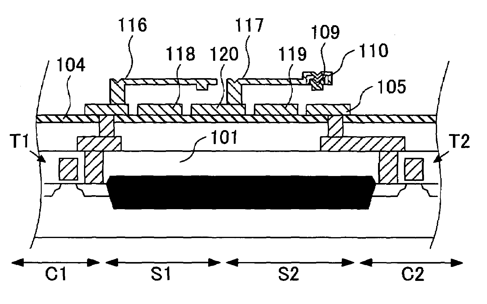
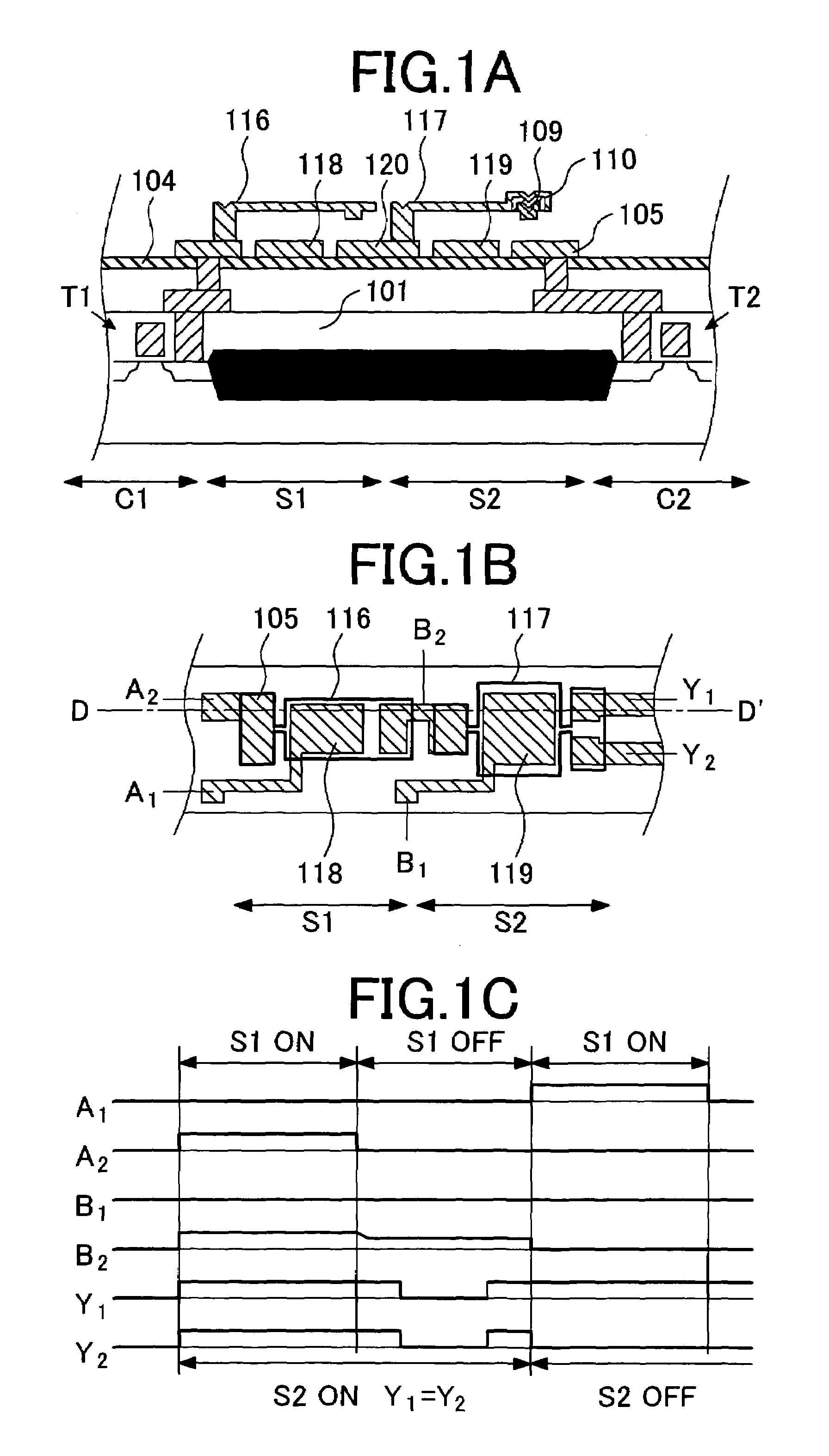
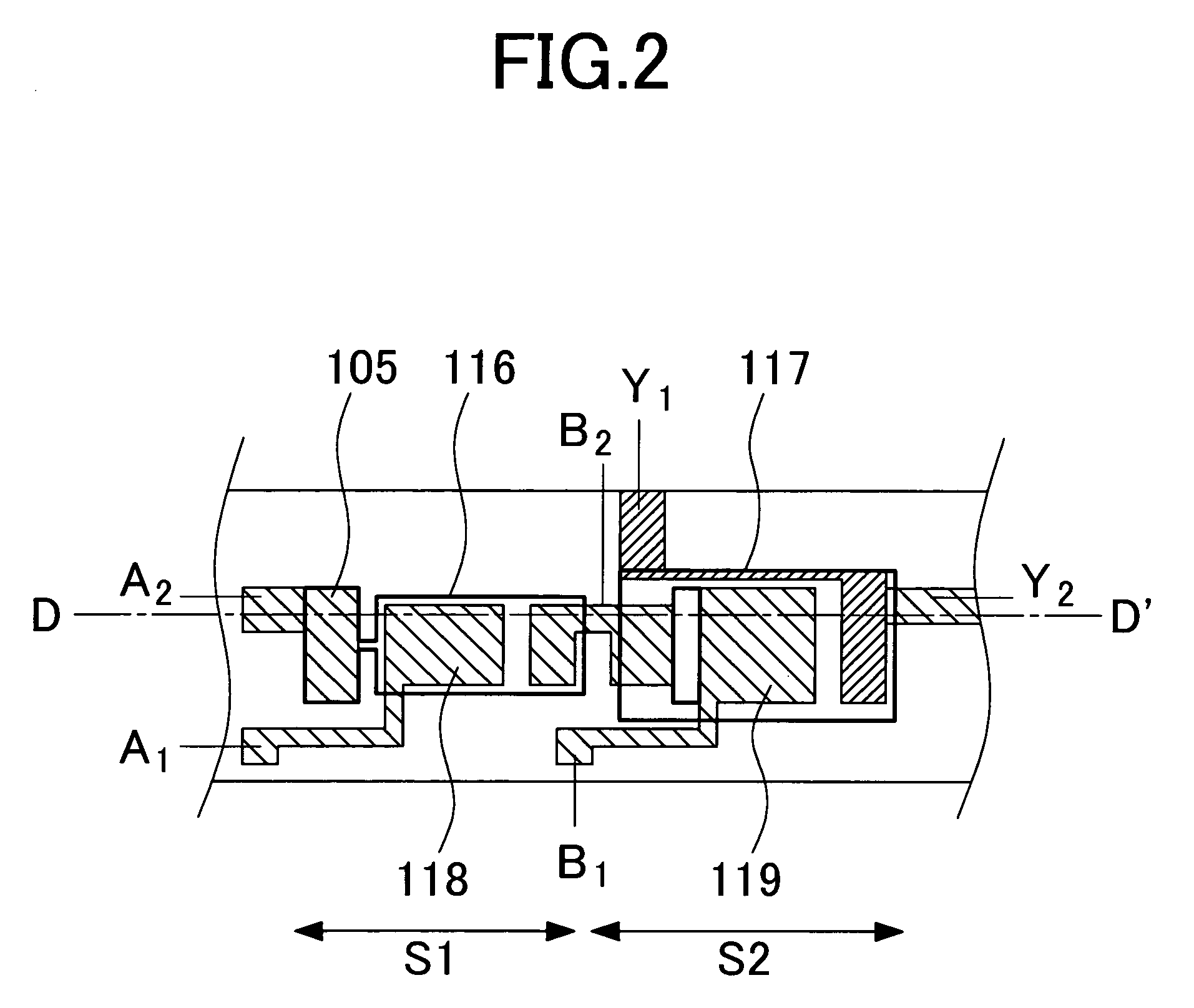
[0030]Referring to FIG. 1, the following describes a MEMS switch device according to a first embodiment of the present invention. FIG. 1A is a section view of the structure of the MEMS switch device according to the present invention while FIG. 1B is a top view of the MEMS switch device. The sectional structure in FIG. 1A is depicted along line D–D′ in FIG. 1B. This MEMS switch is composed of two switches, i.e., a front switch S1 and a rear switch S2. In this embodiment, the front switch S1 is fabricated as a hot switch while the rear switch S2 as a cold switch.

[0031]The hot switch S1 is turned on when a voltage is applied to between two electrodes of a capacitor, a cantilever 116 and a pull-down electrode 118, since the cantilever 116 is attracted toward the pull-down electrode 118 and therefore short-circuited with a contact of signal line 120 (or a stationary contact). In the rear cold switch S2, an insulator 110 is sandwiched between a cantilever 117 and a contact 109 on the can...

embodiment 2

[0055]The following describes a second embodiment of the present invention where a latchable cold switch is realized by using two hot switches.

[0056]Its manufacture process is similar to that shown in FIG. 3 through FIG. 5. FIGS. 7A through 7C show top views of the MEMS switch device. Also in this embodiment, the electrode size of the capacitor to keep the cold switch (S3 in FIG. 7) in the ON or OFF state should be larger than that of the front switches (S1 and S2 in FIG. 7) as mentioned earlier. In the case of the MEMS switch device shown in FIG. 7, all electrodes have the same size. Even such a MEMS switch device can operate reliably if the switch ON voltage is designed comparatively smaller than |Vcc|. FIG. 7A corresponds to FIG. 3B in the progress of process wherein the underlayer metal film is patterned. FIG. 7B corresponds to FIG. 5B in the progress of process and shows the positional relations among an electrode terminal (mobile contact) 109 of the cold switch S3, underlayer ...

embodiment 3

[0061]In the aforementioned first and second embodiments, a latchable MEMS switch device is made by combining one or more hot switches with a cold switch. The same function can also be implemented by combining cold switches. The following describes such a third embodiment of the present invention.

[0062]FIGS. 9A through 9C show an example of a latchable MEMS switch device configured by using three cold switches S1, S2 and S3. FIG. 9B is its top view. FIG. 9A is a cross-sectional view of the structure depicted along line D–D′ in FIG. 9B. FIG. 9C is a timing chart showing its latching mechanism. In this configuration, the switch S3 is a switch with latch function. While the switch S3 is in the ON state, two signal terminals (stationary contacts) Y1 and Y2 are short-circuited with each other (Y1=Y2). While the switch S3 is in the OFF state, the signal terminals Y1 and Y2 are brought into an open-circuit state. How to fabricate this MEMS switch device having cold switches connected in se...


PUM


Abstract

Disclosed herein is a latchable MEMS switch device capable of retaining its ON or OFF state even after the external power source is turned off. It is unnecessary not only to introduce novel materials such as magnetic material but also to form complicated structures. At least one of the cantilever and pull-down electrode of a cold switch is connected to a second MEMS switch. A capacitor between the cantilever and pull-down electrode of the cold switch is charged by the second MEMS switch. Thereafter since the cold switch is isolated in the device, the charge remains stored. Therefore, the cold switch can remain in the ON state since the charge continues to create electrostatic attraction between the cantilever and the pull-down electrode.

Description

FIELD OF THE INVENTION[0001]The present invention relates to semiconductor devices using MEMS (Micro Electro Mechanical System) switches which operate mechanically by converting electrostatic force to actuating force, and more particularly to a semiconductor device using MEMS switches capable of remaining turned on or off even if power from a power source to the MEMS switches is stopped.RELATED ARTS[0002]Due to the progress in lithography technology of semiconductor manufacture, semiconductor devices with design rules of 130 nm to 90 nm are being produced. In addition, the wafer size is advancing from 200 mm to 300 mm in diameter with advancing semiconductor manufacture equipment. Where 300 mm diameter wafers are combined with a design rule of 130 nm or finer, chips are produced in large quantities at a time. In this situation, cell-based system LSI development is not allowed unless the system LSI is expected to be consumed in large quantities. For a user demanding various kinds of ...

Claims


Application Information

Patent Timeline
Patent Type & Authority Patents(United States)
IPC IPC(8): H01L27/108H01L29/76H01L21/82H01H59/00H01L21/00
CPCH01H59/0009H01H2001/0063H01H2001/0042
Inventor GOTO, YASUSHIMACHIDA, SHUNTAROYOKOYAMA, NATSUKI
Owner HITACHI LTD
Why Eureka
Try Eureka