Operating circuit for a dielectrically impeded discharge lamp having an overvoltage protection circuit

a dielectrically impeded discharge lamp and overvoltage protection circuit technology, which is applied in the field of circuits and methods for operating dielectrically impeded discharge lamps, can solve the problems of insufficient monitoring of the voltage across the switching transistor in cases relevant in practice, destruction of the switching transistor, and the overvoltage protection circuit mentioned does not respond quickly enough, etc., to achieve the effect of improving the properties

Active Publication Date: 2006-05-16
PATENT TREUHAND GESELLSCHAFT FUR ELECTRIC GLUEHLAMPEN MBH
View PDF6 Cites 8 Cited by
  • Summary
  • Abstract
  • Description
  • Claims
  • Application Information

AI Technical Summary

Benefits of technology

[0008]The inventor has established that the described monitoring of the voltage across the switching transistor in cases which are relevant in practice is not always sufficient. For example, in particular in the event of higher lamp powers and / or when, depending on the circuitry, a dissipation of the energy stored in the converter inductance takes place in only one of possibly two or more switching transistors, destruction of the switching transistor may result so early that the overvoltage protection circuit mentioned does not respond quickly enough. The invention is therefore directed at preventing any energy which is critical for the switching transistor being built up in the converter inductance before it is established that a lamp has in fact been properly connected. Rather, in a phase which precedes the lamp starting, initially power pulses which are referred to here as test power pulses are applied to the converter. If there is no lamp, the inductance generates a higher induction voltage and thus produces a higher current or a higher power loss in the switching transistor or else a higher voltage drop across the switching transistor than when the lamp is connected, and thus a significant proportion of the energy from the inductance is consumed.
[0009]It should be noted here that, in the individual case, destruction of a switching transistor may result owing to currents, powers or else voltages which are too high. From the point of view of the inventor, it is destruction owing to currents which are too high which is primarily of importance. However, the invention is directed, independently of the precise destruction mechanism, at the protection of the switching transistor against instances of input power which is too “high”. The test power pulses may therefore in the individual case be differentiated from the later starting power pulses or operating power pulses in terms of voltage, current and / or power, depending on the destruction mechanism to be expected.

Problems solved by technology

The inventor has established that the described monitoring of the voltage across the switching transistor in cases which are relevant in practice is not always sufficient.
For example, in particular in the event of higher lamp powers and / or when, depending on the circuitry, a dissipation of the energy stored in the converter inductance takes place in only one of possibly two or more switching transistors, destruction of the switching transistor may result so early that the overvoltage protection circuit mentioned does not respond quickly enough.
If there is no lamp, the inductance generates a higher induction voltage and thus produces a higher current or a higher power loss in the switching transistor or else a higher voltage drop across the switching transistor than when the lamp is connected, and thus a significant proportion of the energy from the inductance is consumed.

Method used


Image

  • Operating circuit for a dielectrically impeded discharge lamp having an overvoltage protection circuit
  • Operating circuit for a dielectrically impeded discharge lamp having an overvoltage protection circuit

Examples


Embodiment Construction

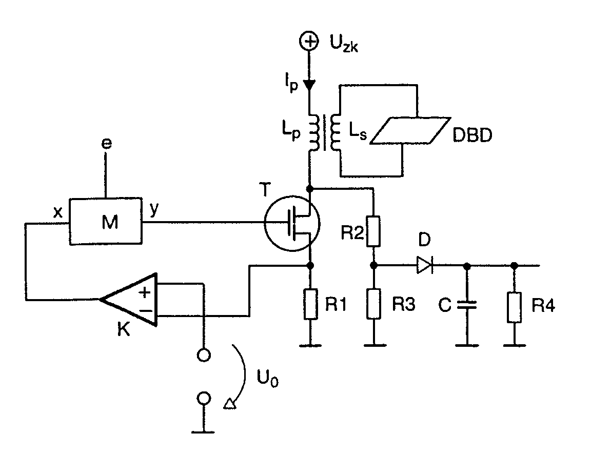
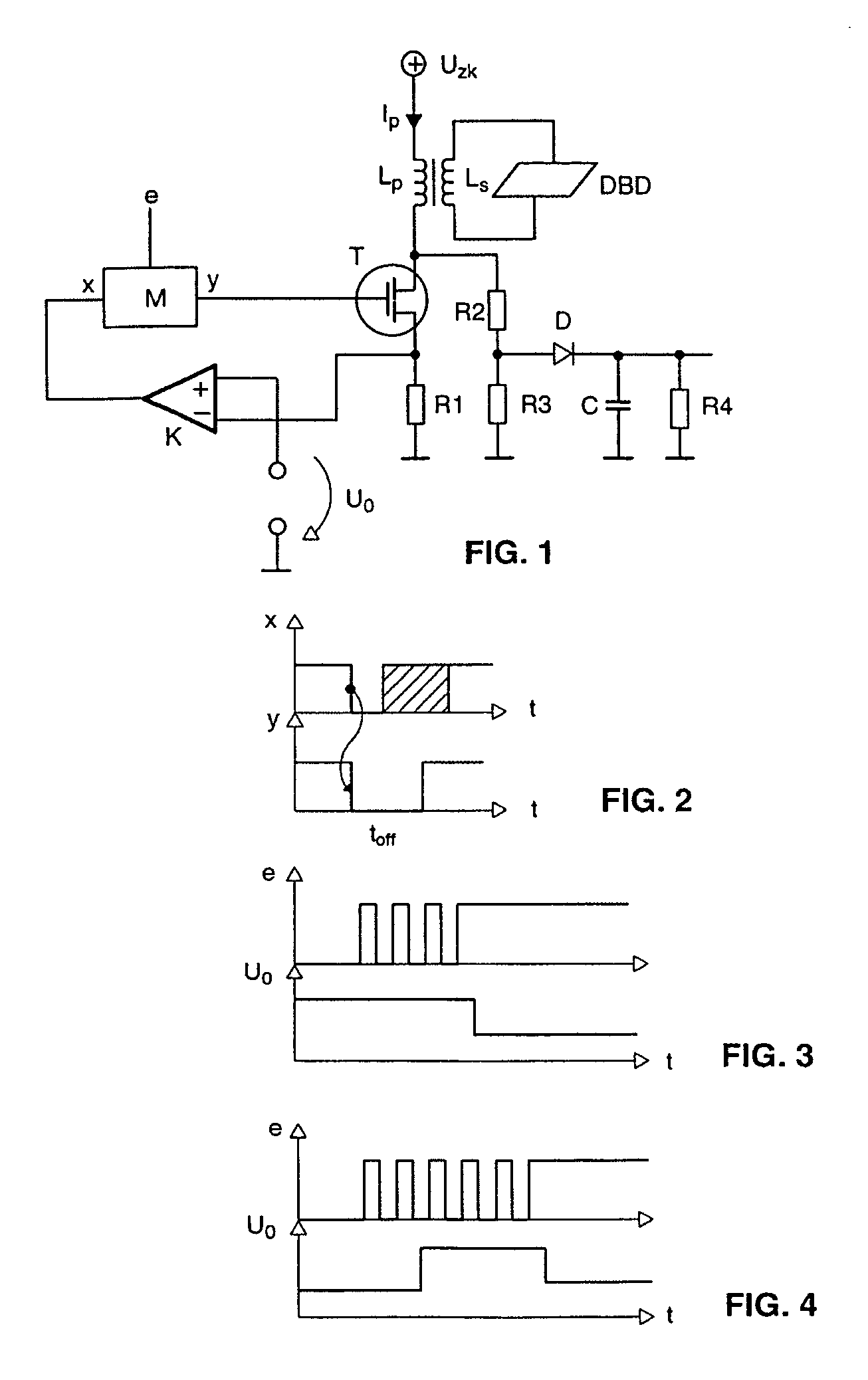
[0023]In FIG. 1, a dielectrically impeded discharge lamp is given the reference DBD and is connected in a secondary circuit to a secondary winding Ls of a transformer. The transformer has a primary winding Lp which has power supplied to it from a voltage source Uzk, the intermediate circuit voltage of a generally known and conventional converter. This induces a flow of current, illustrated by the arrow and the symbol Ip, through the primary winding Lp which then flows to ground via a MOSFET T, connected in series with the primary winding Lp, and a shunt resistor R1. The gate input of the MOSFET switching transistor T which is shown on the left-hand side, is driven by a monoflop M having an input x and an output y and an enable input e. The input x of the monoflop M is in turn driven by a comparator K, at whose positive input a reference voltage U0 is connected to ground, and at whose negative input the voltage between the source connection of the switching transistor T and the shunt...


PUM


Abstract

The invention relates to a method and a circuit for starting or operating discharge lamps which are designed for dielectrically impeded discharges. In this case, it is established in advance, with the aid of an overvoltage protection circuit and test power pulses, whether the discharge lamp is connected.

Description

TECHNICAL FIELD[0001]The present invention relates to a circuit and a method for operating a dielectrically impeded discharge lamp.BACKGROUND ART[0002]Dielectrically impeded discharge lamps are known per se and are largely distinguished by the fact that at least some of the electrodes used for igniting and maintaining the discharge are separated from the discharge medium by a dielectric layer. They are generally also known as “silent discharge lamps”. Such discharge lamps are started and operated using electronic ballasts or, more generally, operating circuits. Higher voltages, and thus higher amplitudes when power is input, are generally required for ignition purposes than during continuous operation.[0003]Operating circuits for such lamps generally contain a converter for inputting the power to the lamp. In principle, such discharge lamps having a very varied AC voltage rating are to be operated, in particular a pulsed mode of operation having power-input phases which are temporal...

Claims


Application Information

Patent Timeline
Patent Type & Authority Patents(United States)
IPC IPC(8): H05B37/02H05B41/26H05B41/24H05B41/28H05B41/288H05B41/292
CPCH05B41/24H05B41/26H05B41/292H05B41/288
Inventor SCHALLMOSER, OSKAR
Owner PATENT TREUHAND GESELLSCHAFT FUR ELECTRIC GLUEHLAMPEN MBH
Why Eureka
Try Eureka