Power up signal generator

a power up signal and generator technology, applied in the direction of electronic switching, automatic control, instruments, etc., can solve the problems of unstable operation of conventional power up signal generators, affecting the operation of the overall memory device, etc., and achieves reduced trip voltage dependence, less influence on trip voltage, and greater consistency

Inactive Publication Date: 2006-05-16
SAMSUNG ELECTRONICS CO LTD
View PDF9 Cites 5 Cited by
  • Summary
  • Abstract
  • Description
  • Claims
  • Application Information

AI Technical Summary

Benefits of technology

[0022]According to an exemplary embodiment of the present invention, a suitable trip voltage of the power up signal generator can be made dependent upon the threshold voltage of a single PMOS transistor in the signal converter and the current source flowing from the trigger node. By reducing the dependency of the trip voltage on MOSFET transistor threshold voltages, the trip voltage can be less affected by changes in operating temperature for the power up signal generator. Therefore, a power up signal generator can provide greater consistency for generating a power up signal in response to changes in temperature.
[0023]According to an exemplary embodiment, the current source includes a reference voltage generator for generating a reference voltage. The amount of current that the current source causes to flow from the trigger node may be dependent on the generated reference voltage, such that the trip voltage of the power up signal generator can be effectively reduced to about the level of a single PMOS transistor threshold voltage. Reducing the trip voltage to such a level helps prevent a power up signal to be disabled (i.e., switched to a low level signal) when the external source voltage drops.

Problems solved by technology

Accordingly, minor fluctuations in the external source voltage VDD that dip below the trip voltage Vtrip may cause the power up signal VccH to switch to a low level, thereby disrupting the operation of the overall memory device.
Accordingly, the trip voltage can be lowered by 400 mV according to an increase of about 100° C. Such sensitivity to temperature can cause unstable operation for conventional power up signal generators.

Method used


Image

  • Power up signal generator
  • Power up signal generator
  • Power up signal generator

Examples


Embodiment Construction

[0029]The present invention and exemplary embodiments thereof are more fully described below with reference to the accompanying drawings. This invention may, however, be embodied in many different forms and should not be construed as being limited to the exemplary embodiments set forth herein; rather, these exemplary embodiments are provided so that this disclosure is thorough and complete, and conveys the concept of the invention to those skilled in the art.

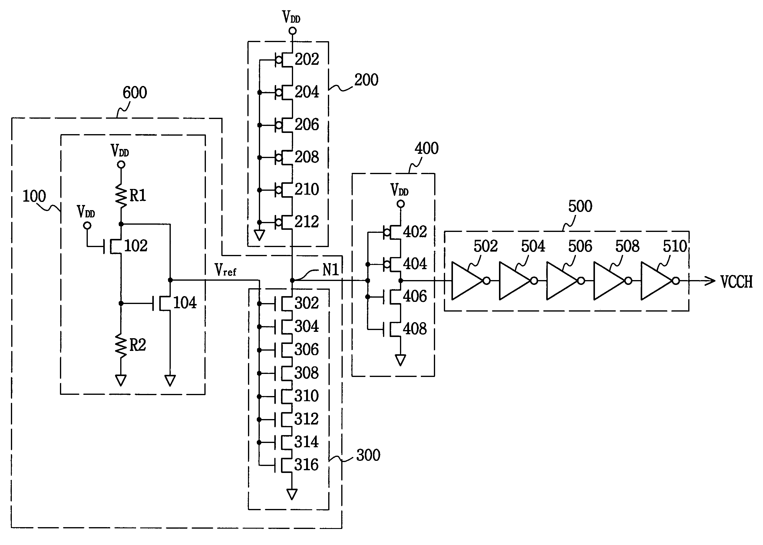
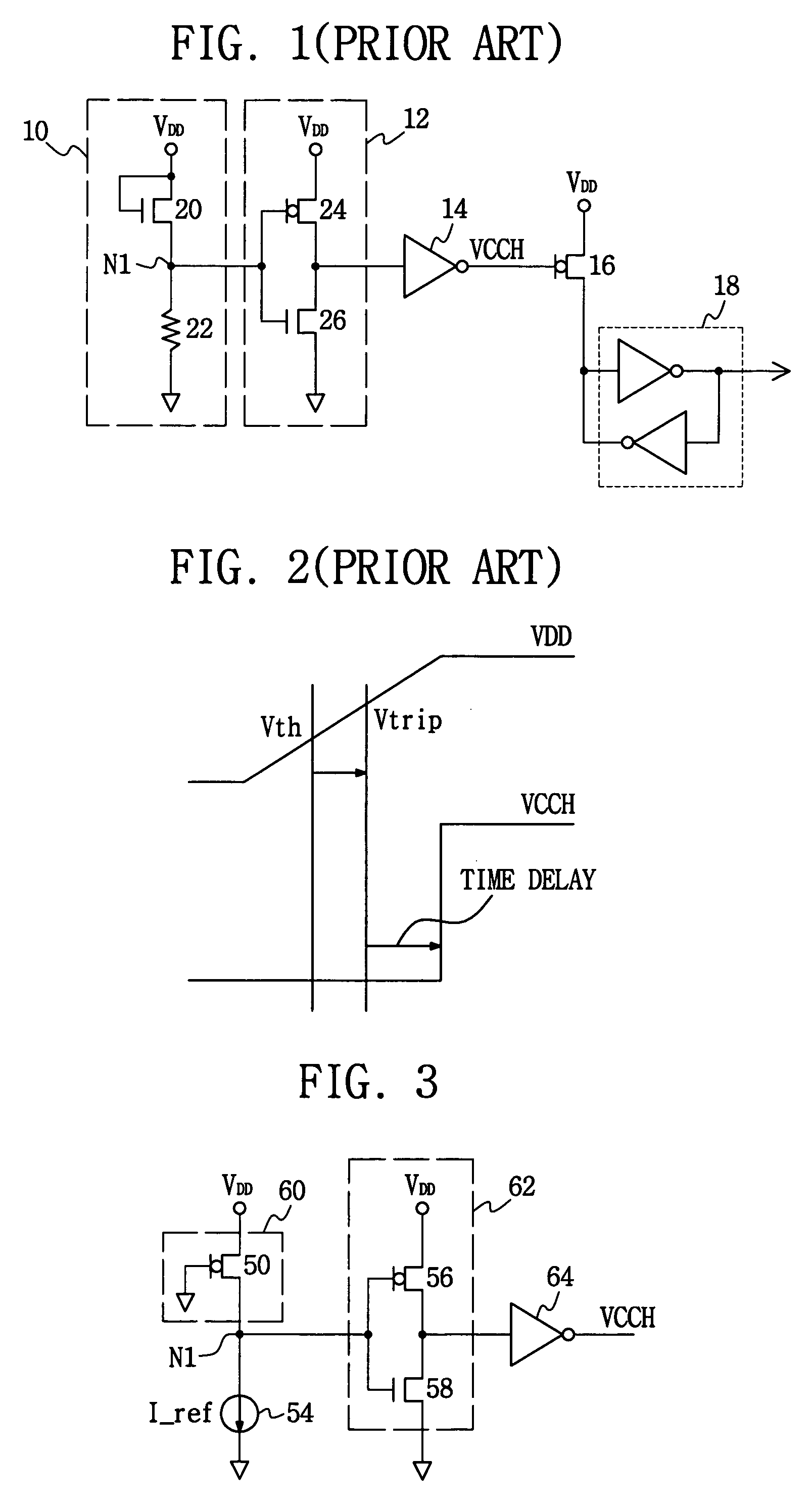
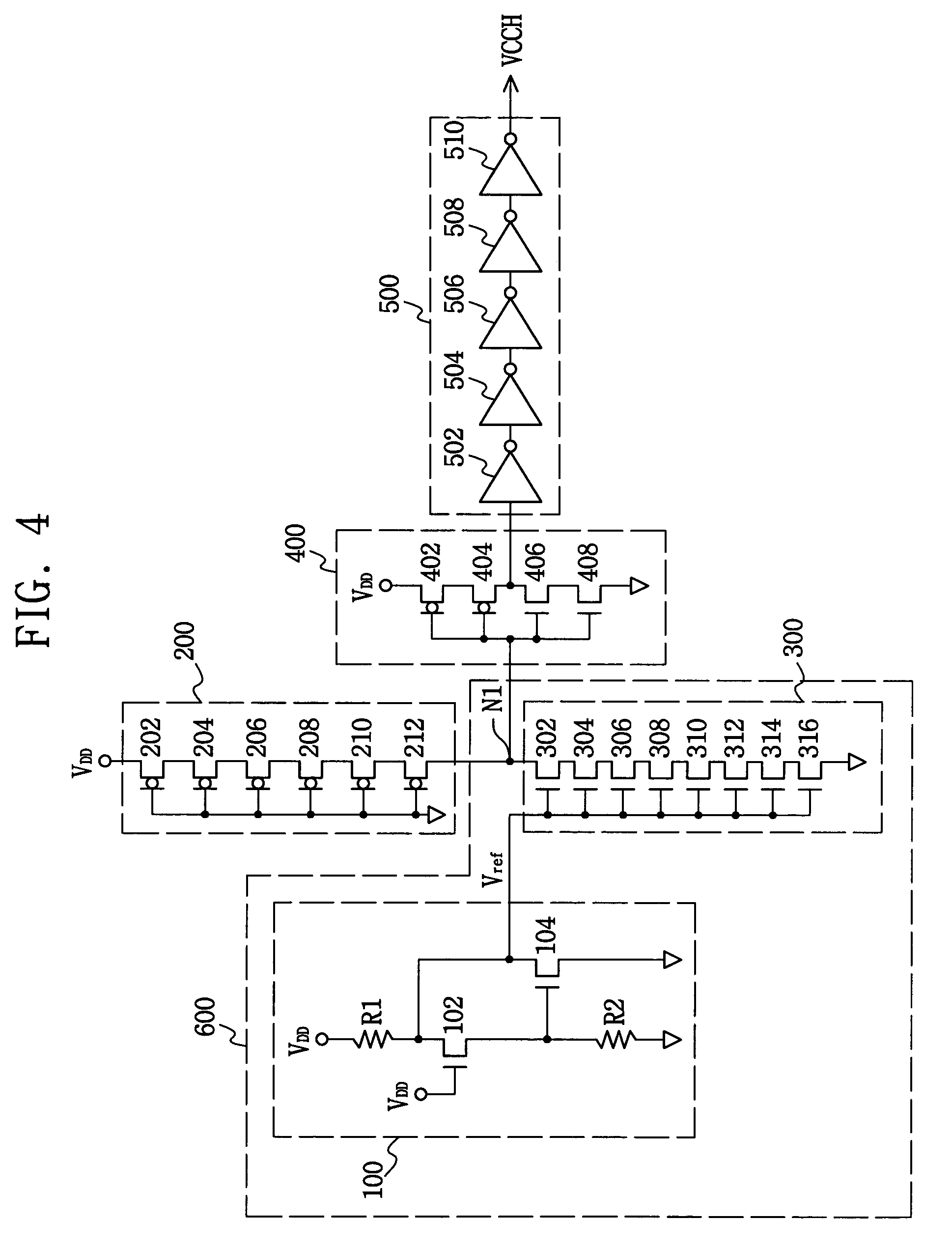
[0030]FIG. 3 is a circuit diagram illustrating a power up signal generator according to an exemplary embodiment of the present invention.

[0031]The power up signal generator of FIG. 3 includes a signal converter 60 for converting the applied external source voltage VDD to an internal signal applied node N1 (sometimes referred to as trigger node) when the external source voltage VDD reaches a threshold. As shown FIG. 3, the signal generator may comprise a PMOS transistor 50, which is positioned between an external source voltage V...


PUM


Abstract

A power up signal generator includes a signal converter for converting an applied external source voltage to a voltage applied at a trigger node when the external source voltage rises to a first threshold, and a current source for flowing a reference current from the trigger node. A first inverter connected to the trigger node outputs a low level signal when the trigger node voltage reaches a second threshold. A second inverter outputs a power up signal after receiving the low level signal from the first inverter. The signal converter may include a PMOS transistor configuration, such that the trip voltage of the power up signal generator is dependent only on a single MOSFET transistor threshold voltage.

Description

[0001]This U.S. nonprovisional patent application claims priority under 35 U.S.C. § 119 of Korean Patent Application 2002-63789 filed on Oct. 18, 2002, the entire contents of which are hereby incorporated by reference.BACKGROUND OF THE INVENTION[0002]1. Field of the Invention[0003]The present invention relates to a power up signal generator, and more particularly, to a power up signal generator with stable operation over a range of operating temperatures.[0004]2. Description of the Related Art[0005]In general, a semiconductor memory device may be equipped with a power up signal generator so that the device is not enabled to operate immediately in response to the application of an external source voltage. Instead, the power up signal generator enables the device to operate after the external source voltage level rises above a threshold. The time required for the external source voltage to reach the threshold can allow for internal circuit components to stabilize at their proper state...

Claims


Application Information

Patent Timeline
Patent Type & Authority Patents(United States)
IPC IPC(8): H03L7/00G11C5/14H03K17/22
CPCH03K17/223G11C5/14
Inventor LIM, KYU-NAM
Owner SAMSUNG ELECTRONICS CO LTD
Why Eureka
Try Eureka