Laminated inductor

a technology of inductance and inductance, which is applied in the direction of inductance, transformer/inductance coil/winding/connection, etc., can solve the problems of increasing the direct-current resistance of the coil b>50/b>, the induct the center value of conductance of each turn cannot be matched to each other, etc., to achieve the effect of very high degree of design freedom

Inactive Publication Date: 2006-05-16
MURATA MFG CO LTD
View PDF6 Cites 59 Cited by
  • Summary
  • Abstract
  • Description
  • Claims
  • Application Information

AI Technical Summary

Benefits of technology

[0008]In order to overcome the problems described above, preferred embodiments of the present invention provide a laminated inductor in which the degree of freedom of design is very high and the most appropriate characteristics can be easily obtained.

Problems solved by technology

However, in the laminated inductor using the conventional spiral coil conductor patterns, since the coil conductor patterns 51 and 52 having a multiple number of turns (two or more turns) are used, the inductance of each turn cannot be adjusted, and accordingly, there was a problem in that the center value of conductance of each turn cannot be matched to each other.
Furthermore, in the conventional laminated inductor, when a necessary inductance cannot be obtained, such countermeasures as the use of coil conductor patterns having many turns, and the use of a material having a high permeability as a laminated body, were taken.
As a result, there was a problem in that the direct-current resistance of the coil 50 increases.
Furthermore, when a material having a high permeability is used as a laminated body, the magnetic saturation occurs in the laminated inductor, and there was a problem in that the direct-current superposition characteristics deteriorate.
In this way, since the number of turns of the coil conductor pattern is restricted in the conventional laminated inductor, there was a problem in that the degree of freedom of design is low and that it is difficult to obtain the most appropriate characteristics.

Method used


Image

  • Laminated inductor
  • Laminated inductor
  • Laminated inductor

Examples


Embodiment Construction

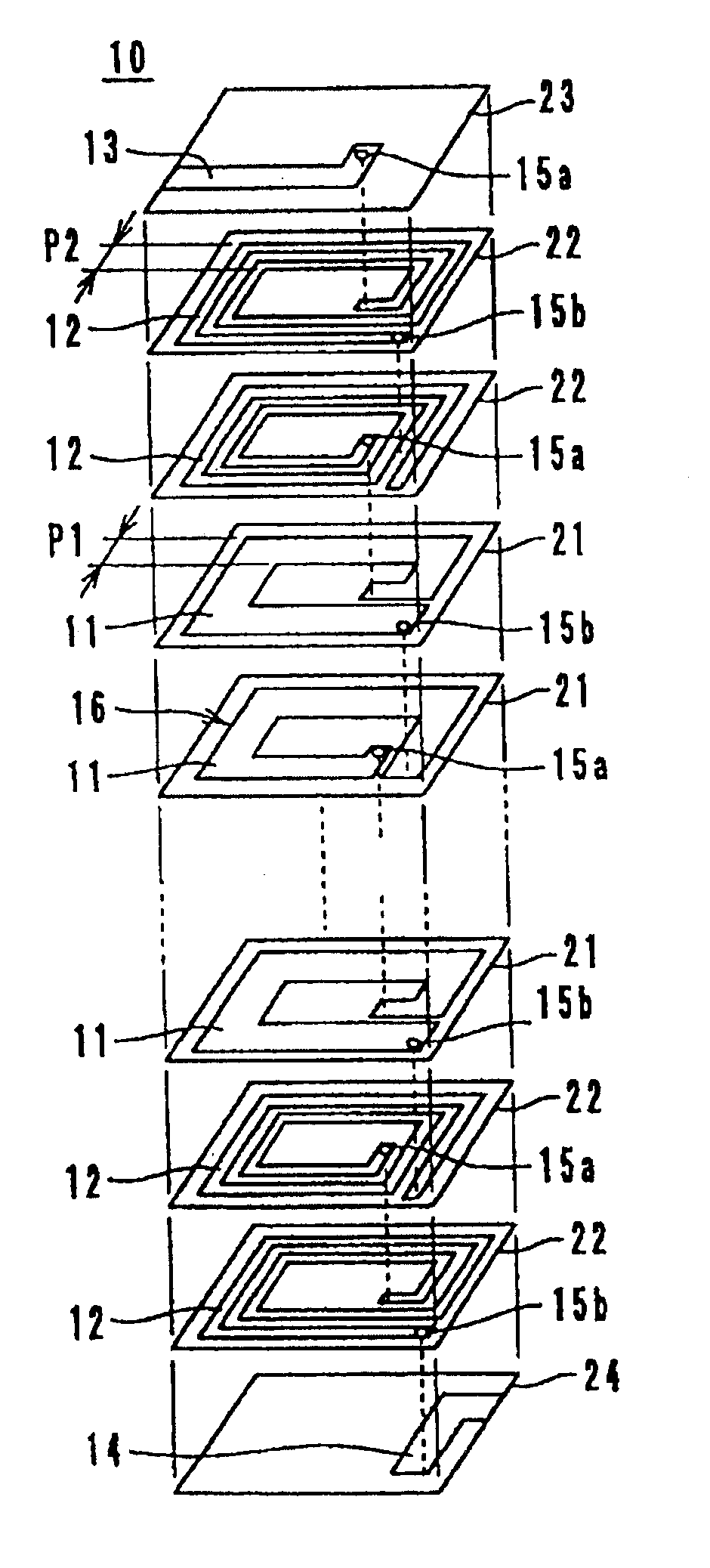
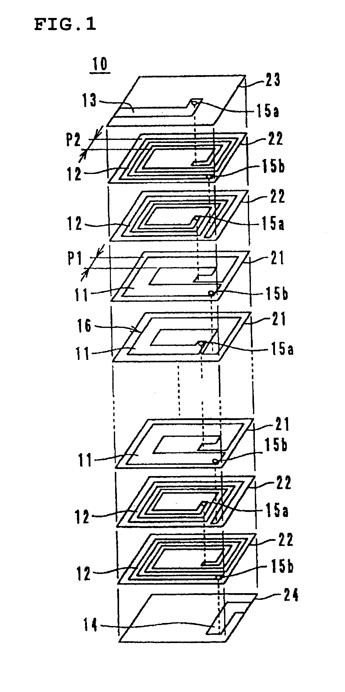
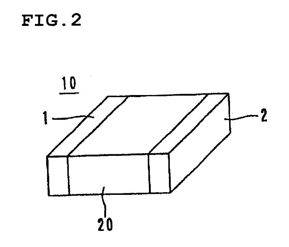
[0023]Hereinafter, preferred embodiments of a laminated inductor according to the present invention are described with reference to the accompanying drawings.

[0024]As shown in FIG. 1, a laminated inductor 10 according to the first preferred embodiment includes of ceramic sheets 21 on each of which a spiral coil conductor pattern 11 constituting one turn is provided, ceramic sheets 22 on each of which a spiral coil conductor pattern 12 constituting two turns is provided, and ceramic sheets 23 and 24 on which lead-out conductor patterns 13 and 14 are provided, respectively. The ceramic sheets 21 to 24 are preferably formed such that a magnetic ceramic powder and a dielectric ceramic powder are mixed and kneaded together with a binder, and other suitable material, and are formed in sheets.

[0025]The ceramic sheets 21 on each of which a spiral coil conductor pattern 11 of one turn is provided are laminated, and the ceramic sheets 22 on each of which a spiral coil conductor pattern 12 of ...


PUM

PropertyMeasurementUnit
inductanceaaaaaaaaaa
widthaaaaaaaaaa
insulatingaaaaaaaaaa

Abstract

A laminated inductor includes ceramic sheets provided with spiral coil conductor patterns of one turn, ceramic sheets provided with spiral coil conductor patterns of two turns, and ceramic sheets provided with lead-out conductor patterns, which are laminated together. The coil conductor patterns are successively electrically connected in series in regular order through via holes. The via holes are disposed at fixed locations in the ceramic sheets.

Description

BACKGROUND OF THE INVENTION[0001]1. Field of the Invention[0002]The present invention relates to a laminated inductor and more particularly, the present invention relates to a laminated inductor for use as a noise filter or other component in, for example, various electronic circuits and apparatuses.[0003]2. Description of the Related Art[0004]Up to now, among such laminated inductors, an inductor in which a coil 50 is disposed inside of a laminated body by connecting spiral coil conductor patterns 51 and 52 in regular order through via holes 53 as shown in FIG. 6 is known. The coil 50 is composed of the coil conductor patterns 51 and 52, each of which constitutes two turns, and the via holes 53. That is, the coil 50 is constructed such that the coil conductor pattern 51 extending in a spiral direction from the outside to the inside and the coil conductor pattern 52 extending in a spiral direction from the inside to the outside are alternately disposed. In this way, the conventional...

Claims


Application Information

Patent Timeline
Patent Type & Authority Patents(United States)
IPC IPC(8): H01F5/00H01F27/245H01F17/00
CPCH01F17/0013H01F27/245
Inventor SAKATA, KEIJI
Owner MURATA MFG CO LTD
Why Eureka
Try Eureka