

Image sensor and image sensor integrated type active matrix type display device
a display device and image sensor technology, applied in the field of active matrix type display devices, can solve the problems of imposing economic burden on users to purchase peripheral devices, deteriorating portability of information processing terminal devices,
- Summary
- Abstract
- Description
- Claims
- Application Information
AI Technical Summary
Benefits of technology
Problems solved by technology
Method used
Image

Examples
embodiment 1
[0061]The embodiment relates to a transmission type liquid crystal display device in which an image sensor and a display matrix are provided on the same substrate.
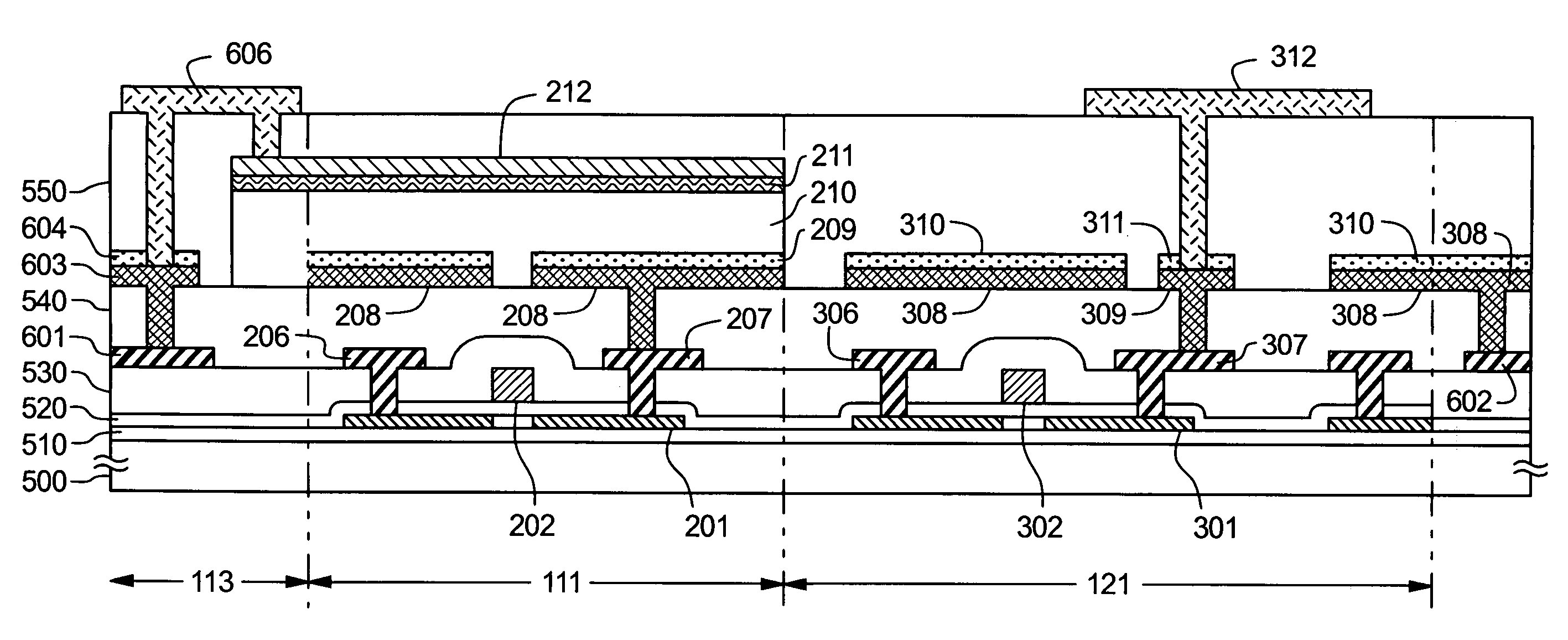
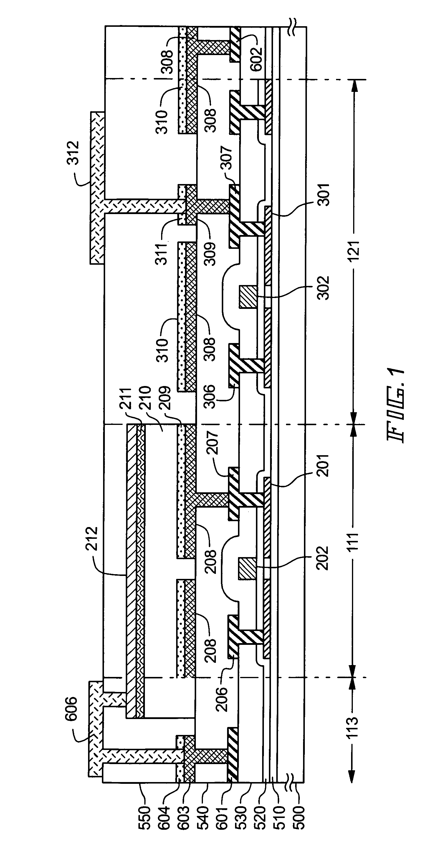
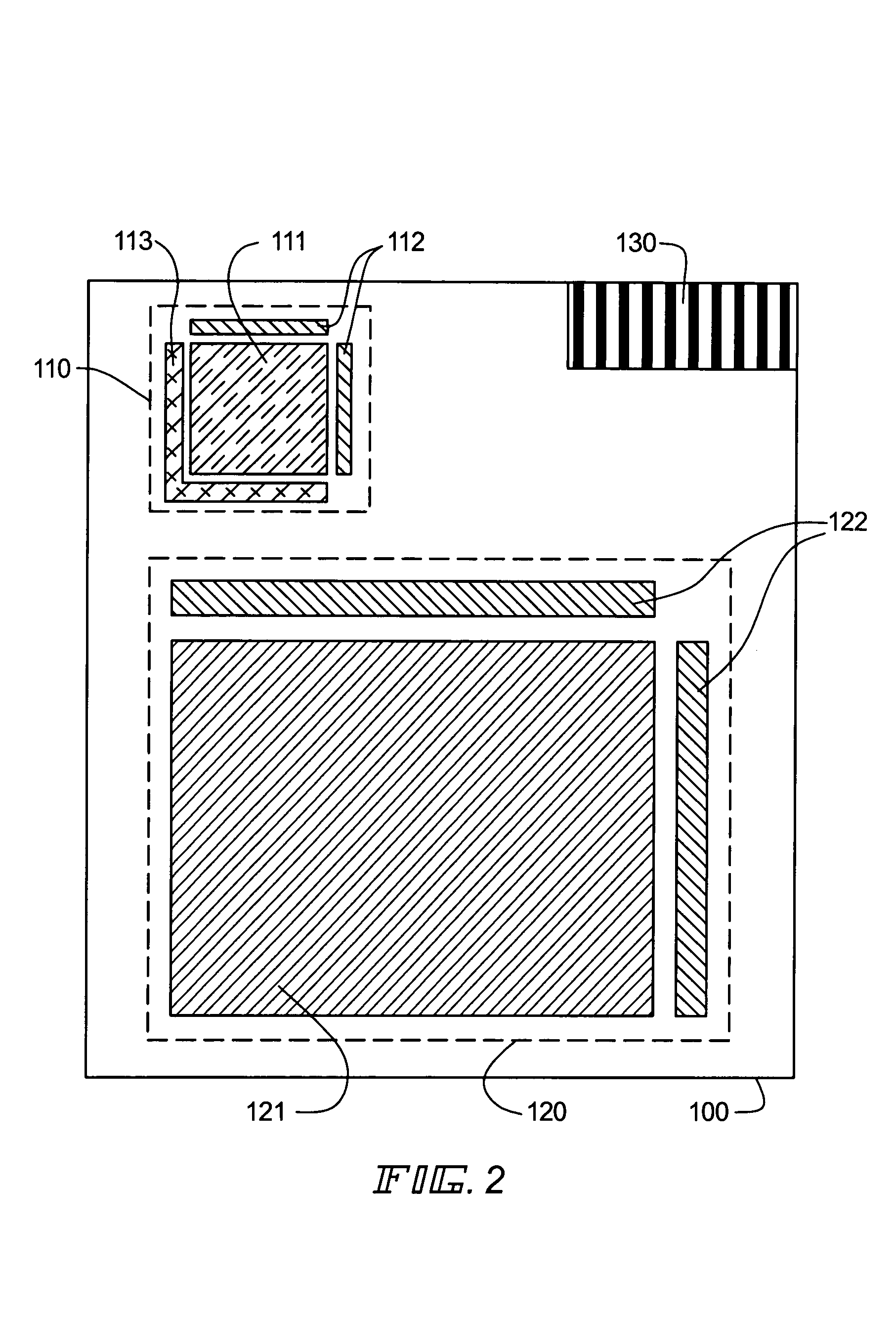
[0062]FIG. 2 is a front view of a liquid crystal display device according to the embodiment. As shown by FIG. 2, both of a light receiving region 110 and a display region 120 are provided on a substrate 100. The light receiving region 110 is formed with the light receiving matrix 111 in which a plurality of light receiving pixels are arranged in a matrix shape, peripheral circuits 112 connected to the light receiving matrix 111 and a terminal unit 113 in which lead-out terminals are arranged to surround portions of the periphery of the light receiving matrix 111 to which the peripheral circuits are not connected. The light receiving matrix 111 is provided with a structure in which a light receiving unit (photodiode) and semiconductor devices for reading electric charge generated at the light receiving unit as signals, are ...
embodiment 2
[0114]The embodiment is a modified example of the terminal unit 113 in the light receiving region 111. An explanation will be given of the embodiment in reference to FIG. 15.
[0115]According to the embodiment, the terminal 601 comprising a starting film the same as that of the signal line 306 is omitted. In this case, a wiring 701 at the lowest layer is constituted by a wiring comprising a starting film the same as that of the electrode layer 308. The shape of the wiring 701 is made similar to that of the terminal 601 of the first embodiment and may be extended to outside of the light receiving matrix 111 to connect to a terminal formed at the outside lead-out terminal unit 130.
embodiment 3
[0116]The embodiment is a modified example of the terminal unit 113 of the light receiving region 111. An explanation will be given of the embodiment in reference to FIG. 16.
[0117]According to the embodiment, the terminal 601, 603 and the layer 604 are omitted. In this case, a wiring 801 arranged at the terminal unit 113 is constituted by only a wiring comprising a starting film the same as that of the pixel electrode 312. The shape of the wiring 801 is similar to the terminal 601 of Embodiment 1 and the wiring 801 may be extended to outside of the light receiving matrix 111 to connect to a terminal formed at the outside lead-out terminal unit 130.
PUM
 Abstract
Description
Claims
Application Information