Light receiving element carrier and optical receiver

a technology of light receiving element and carrier, which is applied in the direction of optical elements, waveguides, instruments, etc., can solve the problems of increasing the cost of the carrier, and increasing the height of the light receiving element carrier, so as to reduce the length of the wiring used for connecting these components with one another, the effect of reducing the heigh

Inactive Publication Date: 2006-05-16
MITSUBISHI ELECTRIC CORP
View PDF2 Cites 10 Cited by
  • Summary
  • Abstract
  • Description
  • Claims
  • Application Information

AI Technical Summary

Benefits of technology

[0013]The present invention is proposed to solve the above-mentioned problems, and it is therefore an object of the present invention to provide a light receiving element carrier that can be reduced in height when it is provided as a module, and an optical receiver including the light receiving element carrier as a module.
[0014]It is another object of the present invention to provide a light receiving element carrier that can be made of cheap alumina, thereby reducing the cost of the light receiving element carrier, and an optical receiver including the light receiving element carrier as a module.
[0015]It is a further object of the present invention to provide a light receiving element carrier that can reduce degradation of its reflection characteristic, and an optical receiver including the light receiving element carrier as a module.
[0032]Accordingly, since the optical fiber can be substantially flush with a plurality of high-frequency terminals mounted on the package housing the light receiving element carrier, the light receiving element carrier can be reduced in height when it is provided as a module as compared with prior art light receiving element carriers.
[0033]In addition, cheap alumina can be used as material of which the light receiving element carrier is made, thereby reducing the cost of the light receiving element carrier.
[0034]Furthermore, since the light receiving element, the preamplifier and the pair of input terminals can be substantially flush with one another, the length of wiring used for connecting these components with one another can be reduced to a minimum. Therefore, the high frequency characteristic can be improved. As a result, degradation of the reflection characteristic of the light receiving element carrier can be reduced.

Problems solved by technology

Thus, cheap alumina cannot be used to form the carrier and therefore the cost of the carrier is increased.
In sum, the first problem encountered in the prior art light receiving element carrier is that the optical fiber is not flush with the electric output terminals and the height of the light receiving element carrier is therefore increased when it is provided as a module.
The second problem is that cheap alumina cannot be used to form the prior art light receiving element carrier and therefore the cost of the carrier is increased.
The third problem is that the reflection characteristic of the prior art light receiving element carrier is deteriorated.

Method used


Image

  • Light receiving element carrier and optical receiver
  • Light receiving element carrier and optical receiver
  • Light receiving element carrier and optical receiver

Examples


embodiment 1

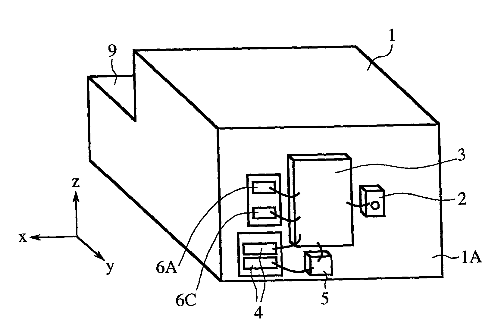
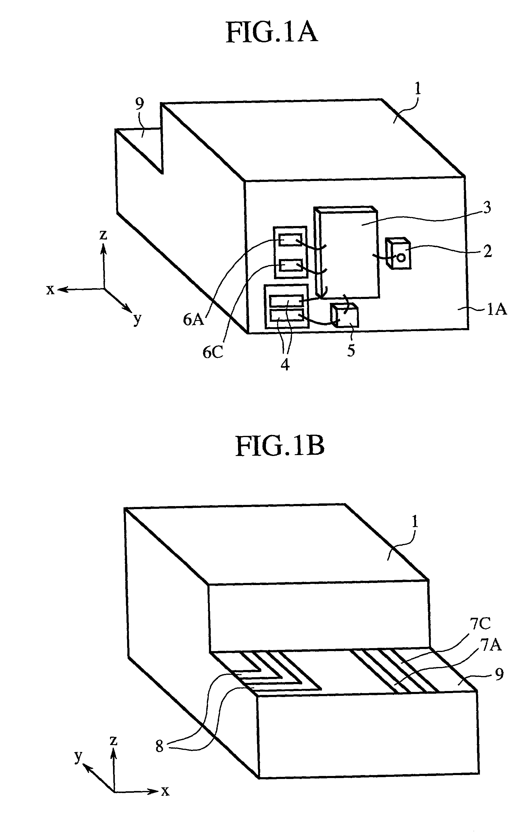
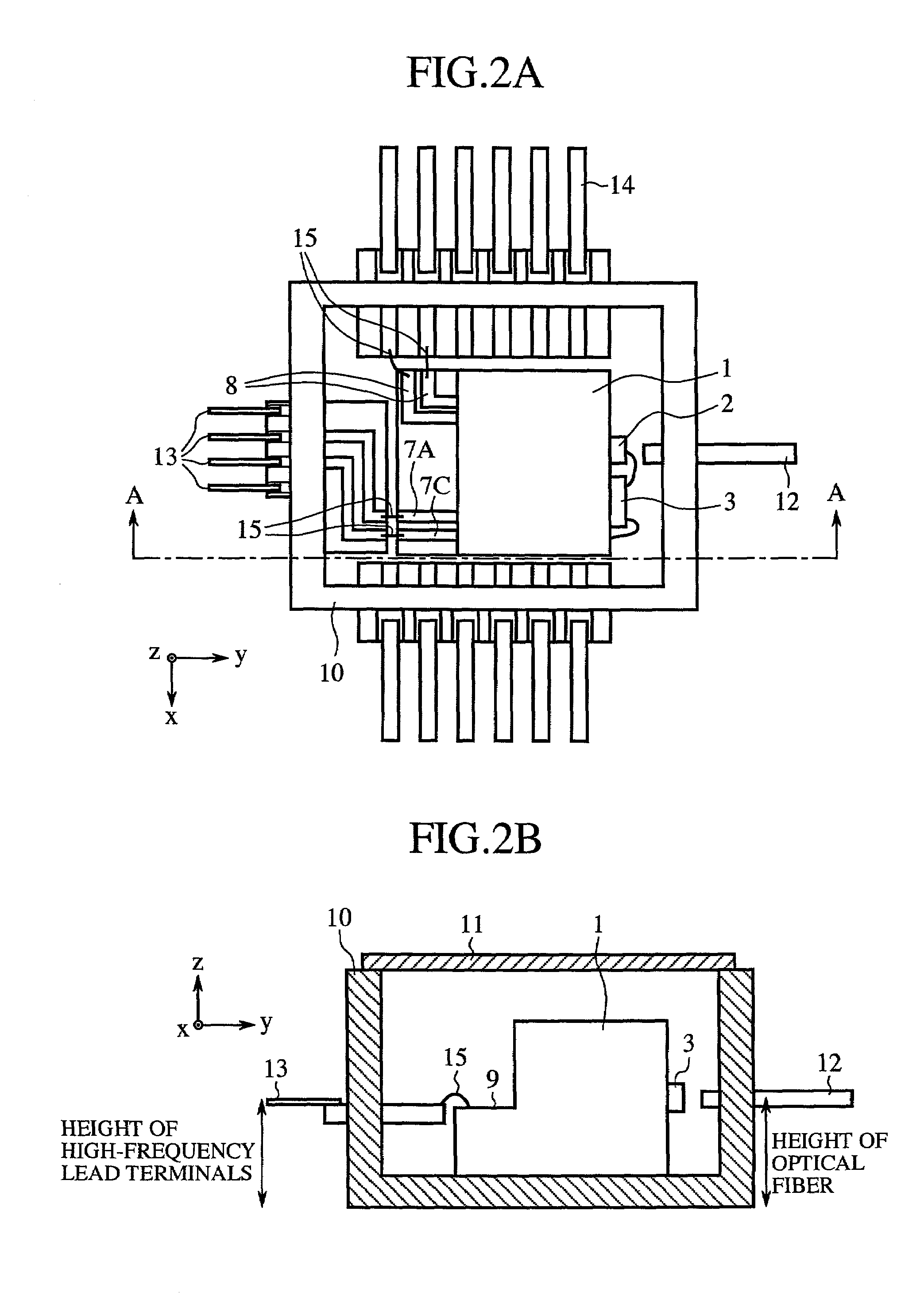
[0047]FIGS. 1A, 1B, 3 and 4A to 4D are views for explaining the structure and features of a light receiving element carrier according to a first embodiment of the present invention, and FIGS. 2A and 2B are views for explaining the structure and features of an optical receiver including the light receiving element carrier. X-, y- and z-axes perpendicular to one another are shown in these figures.

[0048]FIGS. 1A and 1B are perspective views showing the structure of the light receiving element carrier. FIG. 2A is a top plan view showing the optical receiver including the light receiving element carrier as a module when a cover is detached from the optical receiver. FIG. 2B is a partially cross-sectional view taken along the line A—A of FIG. 2A. FIG. 3 is a perspective view showing the structure of high-frequency lines of the light receiving element carrier. Furthermore, FIGS. 4A to 4C are top plan views of the high-frequency lines respectively formed on a first plane A, a second plane B...

embodiment 2

[0066]Referring again to the top plan view of FIG. 2A of the first embodiment, the position where the differential pair of lines 7A and 7C are extending from the carrier 1 is shifted in the direction of the +x-axis with respect to the optical fiber 12. Therefore, there is a necessity to route the differential pair of lines 7A and 7C in the package 10 when the center of the optical fiber 12 needs to be aligned with the center of the corresponding pair of high-frequency lead terminals 13 connected to the differential pair of lines 7A and 7C. In this case, it is necessary to route the two lines for the differential pair of lines 7A and 7C, and therefore an upper area of the optical receiver must be increased. An light receiving element carrier according to a second embodiment of the present invention is so constructed as to solve this problem.

[0067]FIGS. 5 and 6A to 6D are views for explaining the structure and features of the light receiving element carrier according to the second emb...

embodiment 3

[0074]FIG. 7 is a perspective view showing the structure and features of a light receiving element carrier according to a third embodiment of the present invention. In FIG. 7, reference numeral 19 denotes a metallic plate (heat sink) made of a metal of a good thermal conductivity, such as copper tungsten or covar, and used for dissipating heat from a preamplifier 3.

[0075]In the third embodiment, the metallic plate 19 is disposed under a bottom of the preamplifier 3 mounted on the carrier 1. In other words, the preamplifier 3 is installed on a chip mounting surface 1A of the carrier 1 by way of the metallic plate 19 disposed between the chip mounting surface 1A of the carrier 1 and the preamplifier 3. The metallic plate 19 makes it possible for heat generated by the preamplifier 3 to pass through the metallic plate 19 and reach a package 10 within which the carrier 1 is mounted, so that the heat is dissipated.

[0076]Thus, since it is possible to dissipate the heat generated by the pre...


PUM


Abstract

There is provided a light receiving element carrier including first through fourth layers laminated, a differential pair of vertical vias, one of them penetrating the second layer, and the other one of them penetrating the third layer, a broadside-coupled differential pair, one of them being located on a first boundary plane between the first and second layers, for connecting a high-frequency terminal to the one of the differential pair of vertical vias, and the other one of them being located on a third boundary plane between the third and fourth layers, for connecting another high-frequency terminal to the other one of the differential pair of vertical vias, and a differential pair of output lines located on a second boundary plane between the second and third layers, they extending on a terrace portion formed of a surface of the third layer which is partially exposed like a terrace.

Description

BACKGROUND OF THE INVENTION[0001]1. Field of the Invention[0002]The present invention relates to a light receiving element carrier on which a light receiving element, a preamplifier, high-frequency terminals, and so on are mounted. It also relates to an optical receiver including the light receiving element carrier as a module.[0003]2. Description of the Prior Art[0004]FIG. 9 is a perspective view showing the structure of a prior art light receiving element carrier disclosed in Japanese patent application publication (TOKKAI) No. 2000-58881. In FIG. 9, reference numeral 101 denotes a light receiving element, reference numeral 102 denotes a carrier, reference numeral 103 denotes a preamplifier, reference numeral 104 denotes an I / O pad, reference numeral 105 denotes an output pad, reference numeral 106 denotes a Vcc pad, reference numeral 107 denotes a Vee pad, reference numerals 108 to 112 denote carrier electrode patterns, and reference numeral 115 denotes a boding wire for connecti...

Claims


Application Information

Patent Timeline
Patent Type & Authority Patents(United States)
IPC IPC(8): H04B10/06G02B6/42H01L31/0232
CPCG02B6/4201H01L2224/45144H01L2224/48137H01L2924/00H01L2224/05554G02B6/424G02B6/4257G02B6/4274G02B6/4265G02B6/4269
Inventor ARUGA, HIROSHI
Owner MITSUBISHI ELECTRIC CORP
Why Eureka
Try Eureka