Isolating method and transferring method for semiconductor devices

a transfer method and semiconductor technology, applied in the direction of semiconductor devices, basic electric elements, electrical appliances, etc., can solve the problems of difficult removal, difficult to obtain a clean and uniform surface, prolonged exposure period of led devices b>108/b> to etching solution, etc., to achieve high selective etching, uniform and good quality, uniform characteristics

Active Publication Date: 2006-05-23
SONY CORP
View PDF8 Cites 16 Cited by
  • Summary
  • Abstract
  • Description
  • Claims
  • Application Information

AI Technical Summary

Benefits of technology

[0016]Therefore, only a predetermined layer is securely etched away in each of the steps, so that highly selective etching can be achieved, resulting in that the problem that the etching solution exudes to the semiconductor device side in the steps of removing the substrate and the etching stop layer to erode the device portions can be prevented from occurring. In addition, it is possible to achieve device isolation etching which is uniform in plane, so that the shape of each semiconductor device can be made uniform, resulting in that a semiconductor device array with uniform characteristics can be obtained.
[0017]Namely, in the method of isola

Problems solved by technology

However, a thickness of generally about 100 μm of the GaAs substrate 101 is removed by the wet etching, and, therefore, the conventional method as above-mentioned has the problem that the period of time for which the LED devices 108 are exposed to the etching solution is prolonged due to unevenness of etching in plane.
Namely, in the case of the conventional method, the portions where the etching has proceeded faster are exposed to the etching solution until the completion of the etching of the

Method used


Image

  • Isolating method and transferring method for semiconductor devices
  • Isolating method and transferring method for semiconductor devices
  • Isolating method and transferring method for semiconductor devices

Examples


Embodiment Construction

[0047]Now, the method of isolating semiconductor devices and the method of transferring semiconductor devices according to the present invention will be described in detail below, referring to the drawings. In the drawings, for ease of understanding, contraction scales different from the actual contraction scale may be used. The invention is not limited to the following description, and modifications can be appropriately made within the scope of not departing from the gist of the present invention.

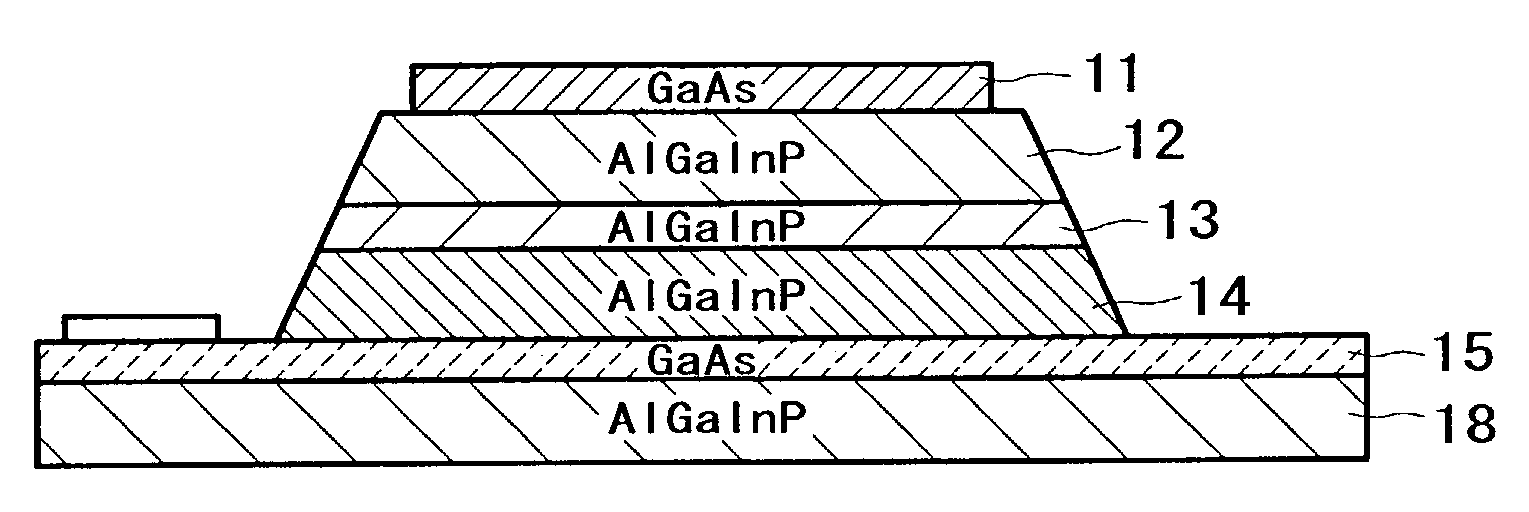
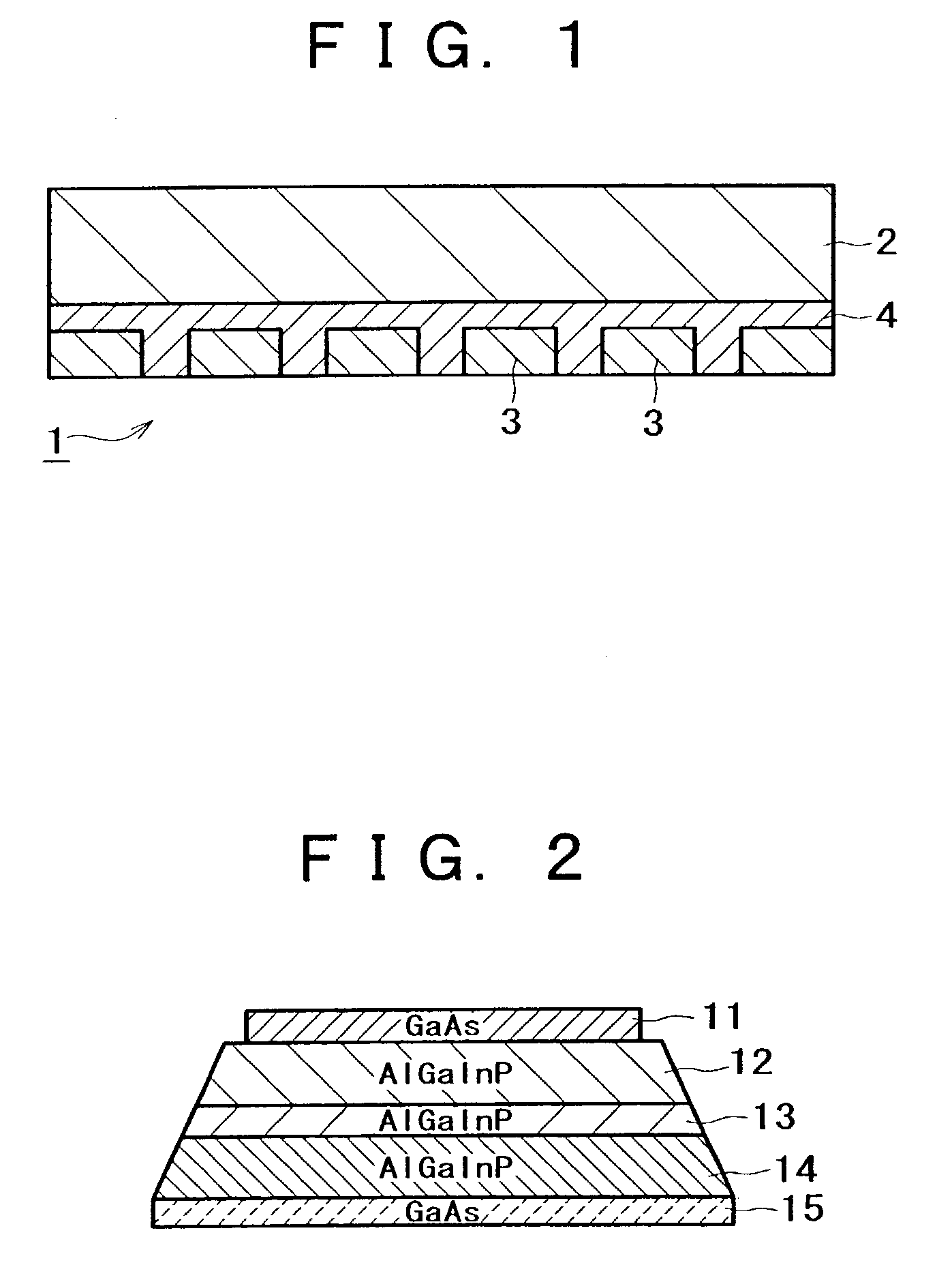
[0048]FIG. 1 is a sectional view showing a micro LED array produced by application of the present invention. The micro LED array 1 (hereinafter referred to simply as LED array 1) has a structure in which micro LED devices 3 (hereinafter referred to simply as LED devices 3) having undergone device isolation are adhered to a transfer substrate 2 by an adhesive layer 4 constituted of an adhesive. Here, each of the LED devices 3 has a structure in which, as shown in FIG. 2, a p-type contact la...


PUM


Abstract

A method of isolating semiconductor devices by wet etching of a semiconductor laminate structure formed on a substrate includes providing an etching stop layer having at least two layers between the substrate and the semiconductor laminate structure. The semiconductor laminate structure is etched to isolate the semiconductor devices, the substrate is then etched away, followed by sequentially etching away of the etching stop layer.

Description

BACKGROUND OF THE INVENTION[0001]The present invention relates to an isolating method and a transferring method for semiconductor devices, and particularly to an isolating method and a transferring method for semiconductor devices which are suitable for application to the manufacture of miniaturized semiconductor devices.[0002]In recent years, a variety of photoelectric devices using a semiconductor material have been developed and put to practical use, and among them are, for example, GaAs-based devices. In the case of forming, for example, a light-emitting diode (hereinafter referred to as LED) array using these GaAs-based devices as photoelectric devices, it is necessary to remove a GaAs substrate in order to provide optical access to the devices.[0003]Here, the conventional method of forming an LED array by use of the GaAs-based devices as photoelectric devices will be described. First, as shown in FIG. 20, a laminate structure 102 for constituting, for example, AlGaInP-based LE...

Claims


Application Information

Patent Timeline
IPC IPC(8): H01L21/30H01L21/46H01L21/302H01L21/306H01L21/308H01L21/461H01L33/08H01L33/20H01L33/30
CPCH01L21/30612H01L21/3083H01L33/0095
Inventor TOMODA, KATSUHIRO
Owner SONY CORP
Why Eureka
Try Eureka