Plasma etching method using gas molecule containing sulfur atom
a sulfur atom and gas molecule technology, applied in the direction of electrical equipment, electrical discharge tubes, chemical instruments and processes, etc., can solve the problems of affecting the underlying etching target, deformation of mask shape, and inability to allow reactions to proceed, so as to achieve high selective etching, less volatile, and easy etching with ions
- Summary
- Abstract
- Description
- Claims
- Application Information
AI Technical Summary
Benefits of technology
Problems solved by technology
Method used
Image
Examples
example 1
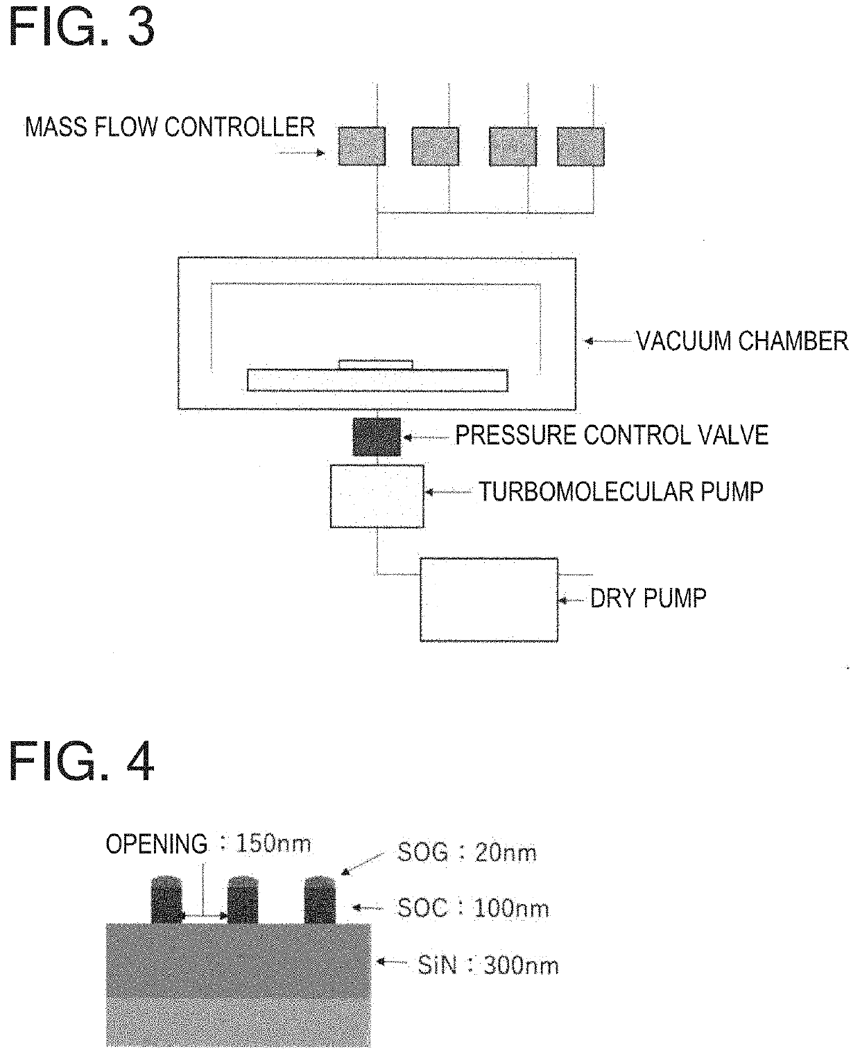
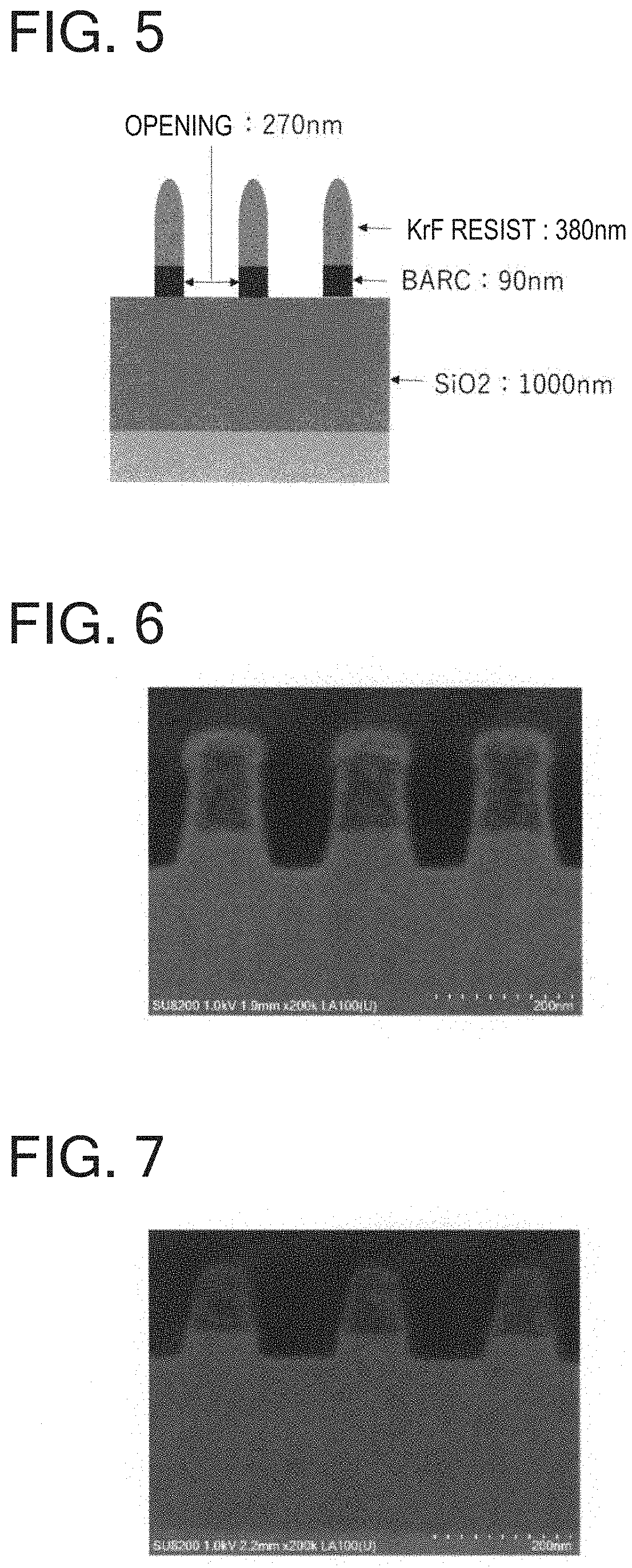
[0098]A plasma was generated under conditions of CH3SCF3: 21.4%, O2: 7.1%, Ar: 71.4%, pressure: 10 Pa, and RF power: 300 W; a SOC / SiN pattern wafer sample was treated with the plasma for a time required for etching the SiN layer by about 50 nm; and the cross-section of the sample was observed with an FE-SEM (FIG. 6). As the etching time, the time for etching SiN by 50 nm is obtained from the etching rate of a SiN blanket wafer calculated in accordance with formula 1 after etching the SiN blanket wafer under the same conditions as the conditions for etching the pattern wafer. The changes in film thickness after etching for the SOG layer, SOC layer, and SiN layer of the pattern wafer were SOG: 11.3 nm, SOC: ±0 nm, and SiN: 56.0 nm. Consequently, selective etching of the SOG and SiN films over the SOC film was possible.
example 2
[0099]A plasma was generated under conditions of CH3SCF3: 23.5%, O2: 17.6%, Ar: 58.8%, pressure: 10 Pa, and RF power: 300 W; a SOC / SiN pattern wafer sample was treated with the plasma for a time required for etching the SiN layer by about 50 nm, and the cross-section of the sample was observed with an FE-SEM (FIG. 7). The changes in film thickness after etching for the SOG layer, SOC layer, and SiN layer of the pattern wafer were SOG: 20.0 nm, SOC: ±0 nm, and SiN: 42.0 nm. Consequently, selective etching of the SOG and SiN films over the SOC film was possible.
example 3
[0106]A plasma was generated under conditions of CHF3: 28.6%, O2: 0%, Ar: 71.4%, pressure: 10 Pa, and RF power: 300 W; a KrF resist / SiO2 pattern wafer was treated with the plasma for a time required for etching the SiO2 by about 300 nm; and the cross-section of the sample was observed with an FE-SEM (FIG. 10). As the etching time, the time for etching SiO2 by 300 nm is obtained from the etching rate of a SiO2 blanket wafer calculated in accordance with formula 1 after etching the SiO2 blanket wafer under the same conditions as the conditions for etching the pattern wafer. The changes from the mask opening width before etching of 270 nm to the opening width of SiO2 after etching (the opening and the bottom of etched SiO2) were assessed (formula 3).
[0107](Formula 3)
[0108]Amount of changes in opening width of SiO2 pattern (hereinafter, ΔWt)=opening width of SiO2 after etching (Wt)−processed width of resist before etching (hereinafter, Wr)
[0109]Amount of changes in bottom width of SiO2 ...
PUM
| Property | Measurement | Unit |
|---|---|---|
| aspect ratio | aaaaa | aaaaa |
| shape | aaaaa | aaaaa |
| volatile | aaaaa | aaaaa |
Abstract
Description
Claims
Application Information


