Phase change memory device

a phase change memory and memory device technology, applied in the direction of static storage, digital storage, instruments, etc., can solve the problems of generating a precise read current of the order of magnitude of 1 a, both during reading and writing, and the complexity of the generation of the precise read current begins to increase, so as to reduce the width of the distribution of resistance values, the effect of simple discrimination and easy reading

Inactive Publication Date: 2006-05-23
STMICROELECTRONICS SRL +1
View PDF7 Cites 99 Cited by
  • Summary
  • Abstract
  • Description
  • Claims
  • Application Information

AI Technical Summary

Benefits of technology

[0023]One embodiment of the invention solves the problem referred to above, reducing the width of the distribution of the resistance values of the phase change cells after writing, so that during reading it will be simpler to discriminate between set cells and reset cells.
[0024]According to one embodiment of the invention, writing of the memory cells takes place by supplying a preset current, according to the desired modification operation, reading of the cells is performed by applying a biasing voltage to the selected cells. In this way, during writing, the topological position of the selected cell does not affect the value of the current flowing in the selected cell and thus in its memory element. During reading, instead, the selected cell is biased by a voltage, thus enabling easier reading and the production of simpler sense circuits.

Problems solved by technology

On the other hand, having wide distributions of cell resistance leads to problems both during reading and during writing.
The generation of a precise read current of the order of magnitude of 1 μA begins to get complicated, in so far as for such values problems arise linked to process variations (mismatch, threshold voltage), temperature variations, etc.

Method used


Image

  • Phase change memory device
  • Phase change memory device
  • Phase change memory device

Examples


Embodiment Construction

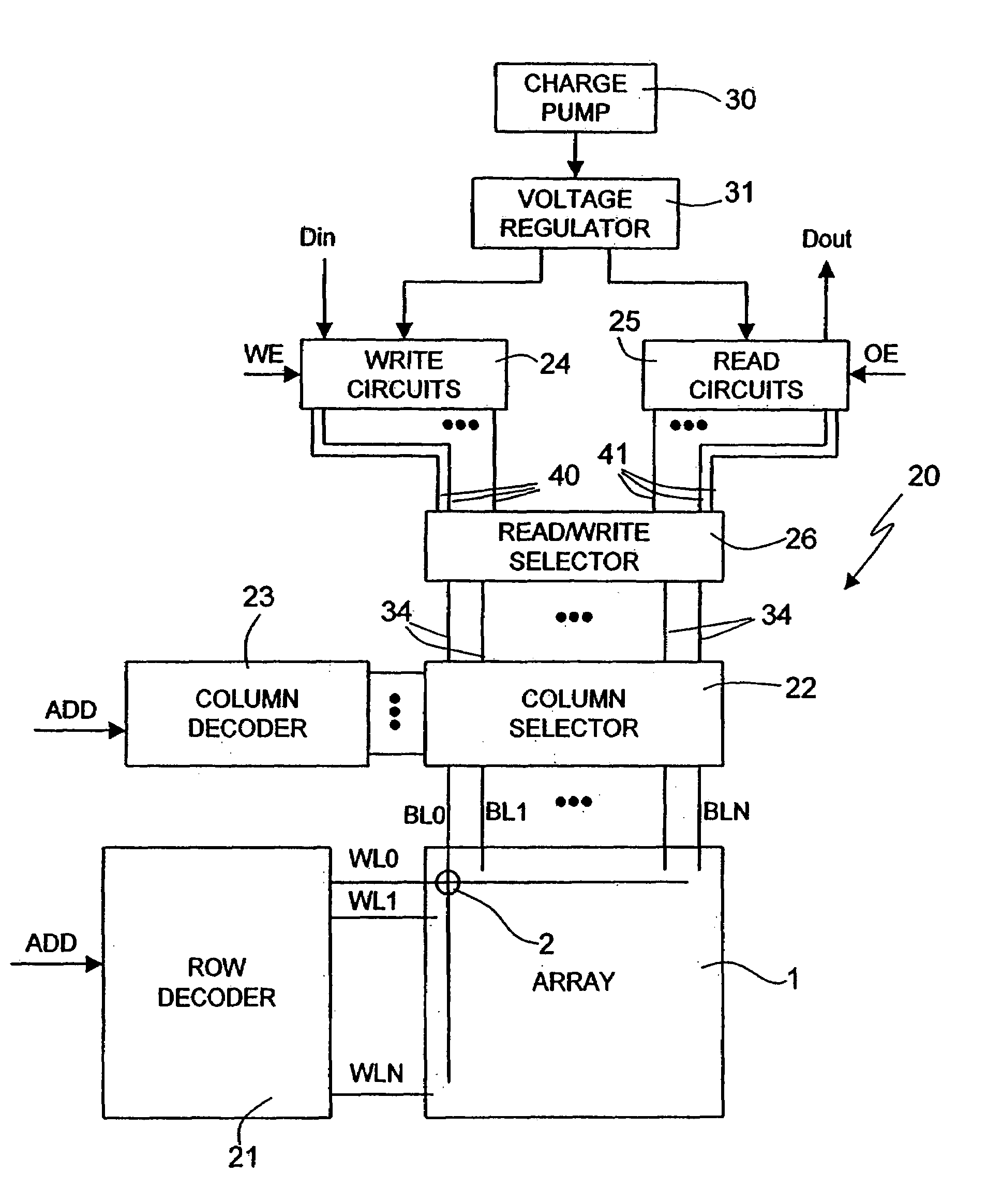
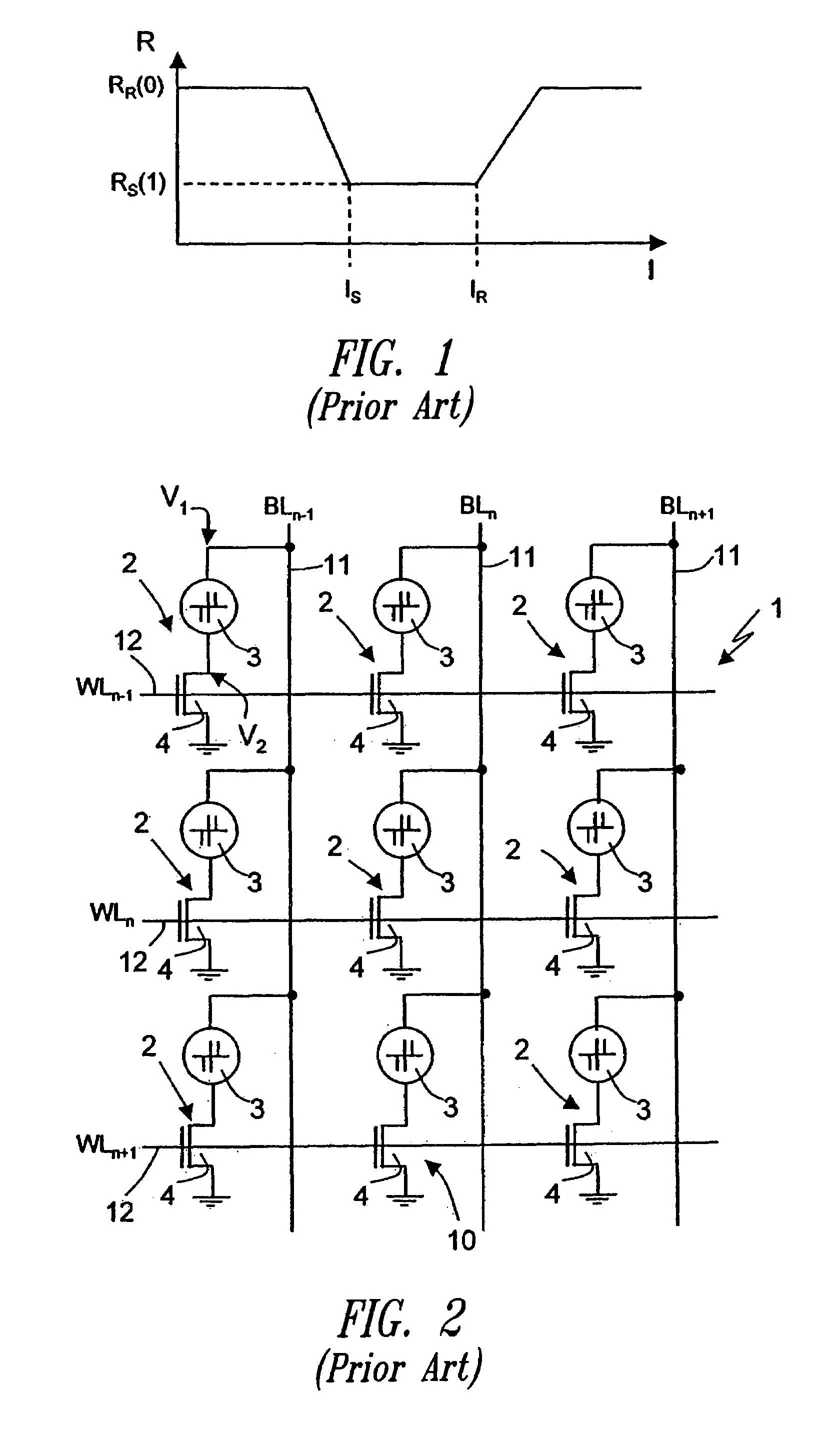
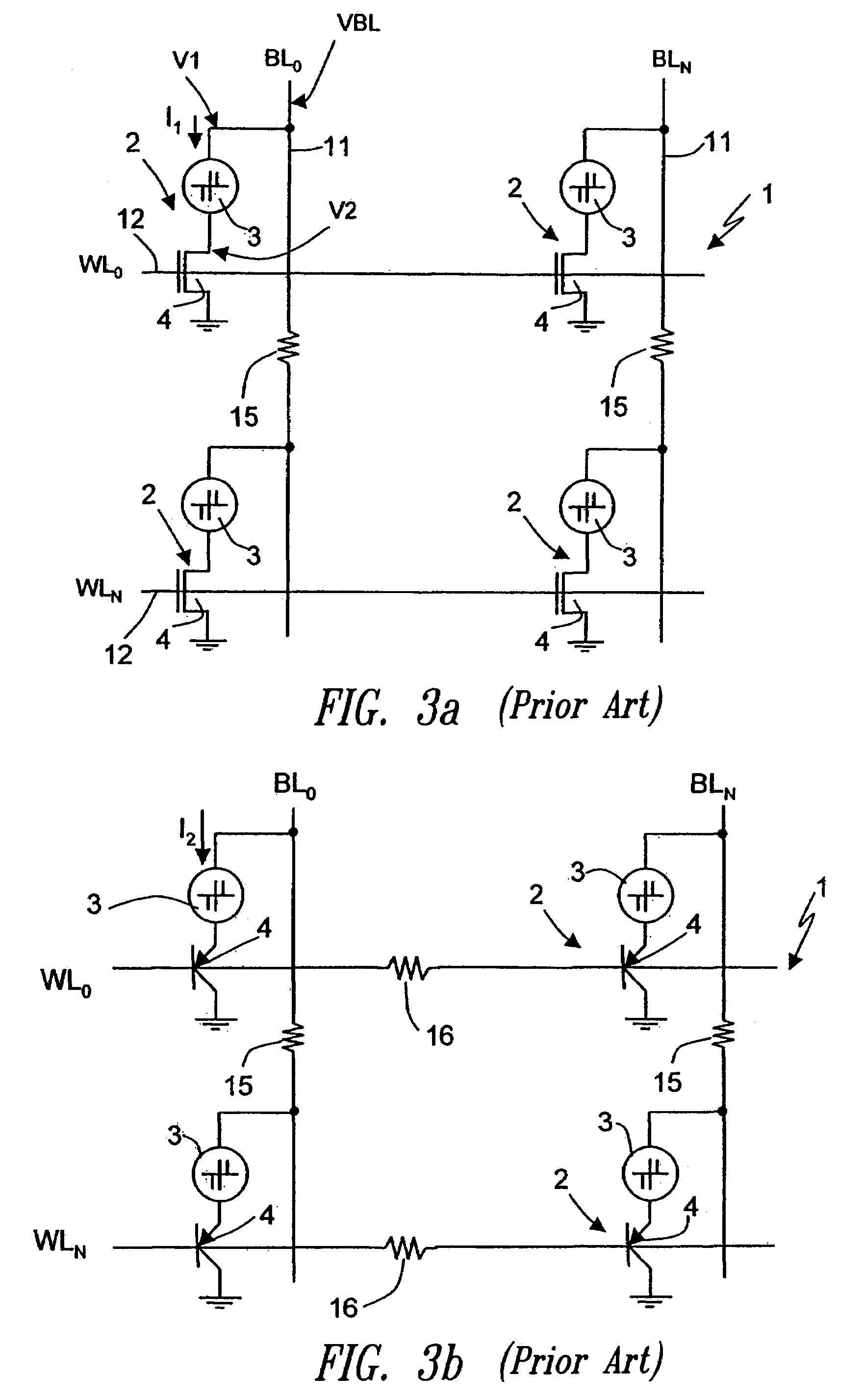
[0040]According to FIG. 4, a phase change memory (PCM) device 20 comprises a memory array 1 having the structure illustrated in FIGS. 2 and 3a or 3b, the cells 2 whereof (only one shown in a schematic way) are addressed through wordlines WL0, WL1, . . . , WLN extending from a row decoder 21 and through bitlines BL0, BL1, . . . , BLN, extending from a column selector 22, illustrated in greater detail in FIG. 5 and controlled by column selection signals supplied by a column decoder 23.

[0041]The column selector 22 is moreover selectively connected to a write stage 24 or to a read stage 25 through a read / write selector 26, shown in detail in FIG. 5. The write stage 24 (described in greater detail hereinbelow) generates the currents necessary for writing. To this end, it receives a write enable signal WE and input data Din, and supplies currents of appropriate value to the column selector 22. The latter supplies these currents to the bitlines BL selected according to the column selection...


PUM


Abstract

A phase change memory has an array formed by a plurality of cells, each including a memory element of calcogenic material and a selection element connected in series to the memory element; a plurality of address lines connected to the cells; a write stage and a reading stage connected to the array. The write stage is formed by current generators, which supply preset currents to the selected cells so as to modify the resistance of the memory element. Reading takes place in voltage, by appropriately biasing the selected cell and comparing the current flowing therein with a reference value.

Description

BACKGROUND OF THE INVENTION[0001]1. Field of the Invention[0002]The present invention relates to a phase change memory (PCM) device.[0003]2. Description of the Related Art[0004]As is known, phase change memory arrays are based upon memory elements which use a class of materials that have the property of switching between two phases having distinct electrical characteristics, associated to two different crystallographic structures of the material forming the memory element, and precisely an amorphous, disorderly phase and a crystalline or polycrystalline, orderly phase. The two phases are hence associated to resistivities of considerably different values.[0005]Currently, the alloys of elements of group VI of the periodic table, such as Te or Se, referred to as calcogenides or calcogenic materials, can be used advantageously in phase change memory cells. The currently most promising calcogenide is formed from an alloy of Ge, Sb and Te (Ge2Sb2Te5), which is now widely used for storing ...

Claims


Application Information

Patent Timeline
Patent Type & Authority Patents(United States)
IPC IPC(8): G11C11/00G11C13/00G11C11/56G11C16/02G11C16/28G11C16/30
CPCG11C11/56G11C11/5678G11C13/0004G11C13/0064G11C13/0069G11C13/0038G11C2213/79G11C2013/0054
Inventor KHOURI, OSAMARESTA, CLAUDIO
Owner STMICROELECTRONICS SRL
Why Eureka
Try Eureka