Memory device and manufacturing method thereof

A technology of memory element and manufacturing method, which is applied in the fields of semiconductor/solid-state device manufacturing, electrical components, electric solid-state devices, etc., can solve the problems of poor electrical performance of memory cells, increased distribution width of memory cells, unstable gate coupling rate, etc. , to achieve stable gate coupling rate, narrow distribution width, and avoid bird's beak effect

Active Publication Date: 2021-10-12
POWERCHIP SEMICON MFG CORP
View PDF5 Cites 0 Cited by
  • Summary
  • Abstract
  • Description
  • Claims
  • Application Information

AI Technical Summary

Problems solved by technology

Based on this, there will be an unstable gate coupling ratio between the control gate and the floating gate filled in the groove, and the distribution width of the threshold voltage of the memory cell is also significantly increased, which also causes the memory cell to have poor performance. electrical performance

Method used


Image

  • Memory device and manufacturing method thereof
  • Memory device and manufacturing method thereof
  • Memory device and manufacturing method thereof

Examples


Embodiment Construction

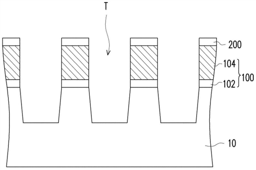
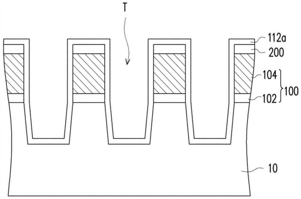
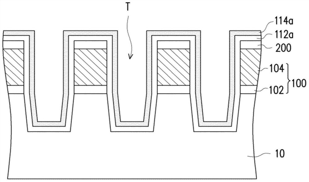
[0050] Figure 1A to Figure 1J is a schematic diagram of a method of manufacturing a memory element according to an embodiment of the present invention.

[0051] Please refer to Figure 1A , firstly, a substrate 10 is provided. The substrate 10 is, for example, a semiconductor substrate, a semiconductor compound substrate, or a semiconductor over insulator (SOI) on a dielectric layer. The aforementioned semiconductors are, for example, atoms of group IVA, such as silicon or germanium. The aforementioned semiconductor compound is, for example, a semiconductor compound formed of atoms of group IVA, such as silicon carbide or silicon germanium, or a semiconductor compound formed of atoms of group IIIA and group VA, such as gallium arsenide.

[0052] Please continue to refer to Figure 1A, and then, forming a plurality of stacked structures 100 on the substrate 10 . In this embodiment, each stack structure 100 includes a tunneling dielectric layer 102 and a floating gate 104 ....


PUM


Abstract

The invention discloses a memory device and a manufacturing method of the memory device. The manufacturing method includes steps below. A plurality of stack structures including a tunneling dielectric layer and a floating gate are formed on a substrate. A liner material layer including a nitride liner layer is formed on the substrate. A top surface of the nitride liner layer is lower than a top surface of the floating gate and is higher than a top surface of the tunneling dielectric layer. An isolation material layer covering the liner material layer is formed on the substrate. The isolation material layer is oxidized, and a portion of the isolation material layer is removed to form an isolation structure. An inter-gate dielectric layer covering the stack structures and the isolation structure is formed on the substrate. A control gate covering the inter-gate dielectric layer is formed on the substrate.

Description

technical field [0001] The present invention relates to a semiconductor element and its manufacturing method, and in particular to a memory element and its manufacturing method. Background technique [0002] A typical memory element is generally designed to have a structure of a plurality of memory cells, wherein each memory cell includes a tunnel dielectric layer, a floating gate, an inter-gate dielectric layer and a control gate sequentially disposed on the substrate, In addition, an isolation structure is provided between adjacent memory cells. In the manufacturing process of the isolation structure, a flowable isolation material layer is usually formed first, and then an oxidation process and an etching process are performed on the isolation material layer. The above-mentioned oxidation manufacturing process can make the formed isolation structure include a higher proportion of oxygen atoms to have a good isolation effect; however, the oxygen introduced in the oxidation...

Claims


Application Information

Patent Timeline
Patent Type & Authority Applications(China)
IPC IPC(8): H01L27/11517H01L21/762
CPCH01L21/76224H10B41/00H01L29/40114H01L29/42336H10B41/30H01L29/7883H01L29/66825
Inventor 杨文忠陈仕锡林威璋
Owner POWERCHIP SEMICON MFG CORP
Why Eureka
Try Eureka