Microelectronic packages with self-aligning features

a technology of microelectronic components and features, applied in the direction of printed circuits, semiconductor devices, semiconductor/solid-state device details, etc., can solve the problems of increasing the overall size of the package, complicating the task of handling and feeding the stacked packages, and affecting the placement of the packages, so as to reduce the number of metallic layers required and simplify the routing of the traces

Inactive Publication Date: 2006-05-30
TESSERA INC
View PDF104 Cites 74 Cited by
  • Summary
  • Abstract
  • Description
  • Claims
  • Application Information

AI Technical Summary

Benefits of technology

[0014]A further aspect of the present invention provides a microelectronic package comprising an elongated substrate such as an elongated strip having a proximal part, a distal part and a central part disposed between the proximal and distal parts. The package includes a microelectronic device mounted to one of these parts. The substrate is folded so that the proximal and distal parts overlie the central part, and so that the microelectronic device disposed between the central part and at least one of the proximal and distal parts. For example, the microelectronic device may be mounted on the central part and both the proximal and distal parts may overlie the microelectronic device. The substrate has a proximal set of traces extending along the substrate from the central part to the proximal part and has a distal set of traces extending along the substrate from the central part to the distal part. Thus, in the folded condition, the traces extend across folds on opposite sides of the structure. The substrate desirably has a set of central terminals disposed on the central part, a set of proximal terminals disposed on the proximal part and a set of distal terminals disposed on the distal part. In the folded condition, the proximal and distal terminals desirably form an array of terminals on one side of the package. The proximal set of traces connects at least some of said proximal terminals with at least some of the central terminals, with the microelectronic device, or both, whereas the distal set of traces connects the distal terminals with at least some of said central terminals, with the microelectronic device, or both. The use of two sets of traces extending across two separate folds to connect the array of terminals with the remainder of the package greatly simplifies routing of the traces. This can reduce the number of metallic layers required in the substrate. Most preferably, the substrate includes only a single layer of traces.

Problems solved by technology

However, inaccuracies in folding the substrate can cause parts of the package to lie in positions different from its nominal position relative to the mounting terminals.
This effectively increases the overall size of the package.
Moreover, the piece-to-piece differences between nominally identical packages caused by folding inaccuracies can complicate the task of handling and feeding the stacked packages during automated assembly operations as, for example, during mounting to the circuit panel.
Also, displacement of the connecting terminals from their nominal position can complicate the tasks of connection an additional element to the connection terminals and the task of engaging the connecting terminals with a test fixture during a testing operation.

Method used


Image

  • Microelectronic packages with self-aligning features
  • Microelectronic packages with self-aligning features
  • Microelectronic packages with self-aligning features

Examples


Embodiment Construction

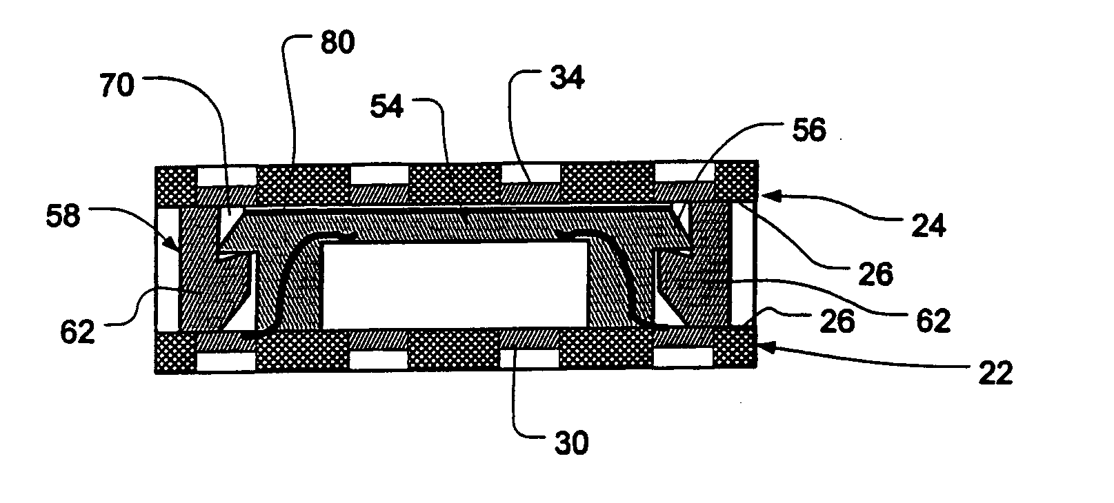
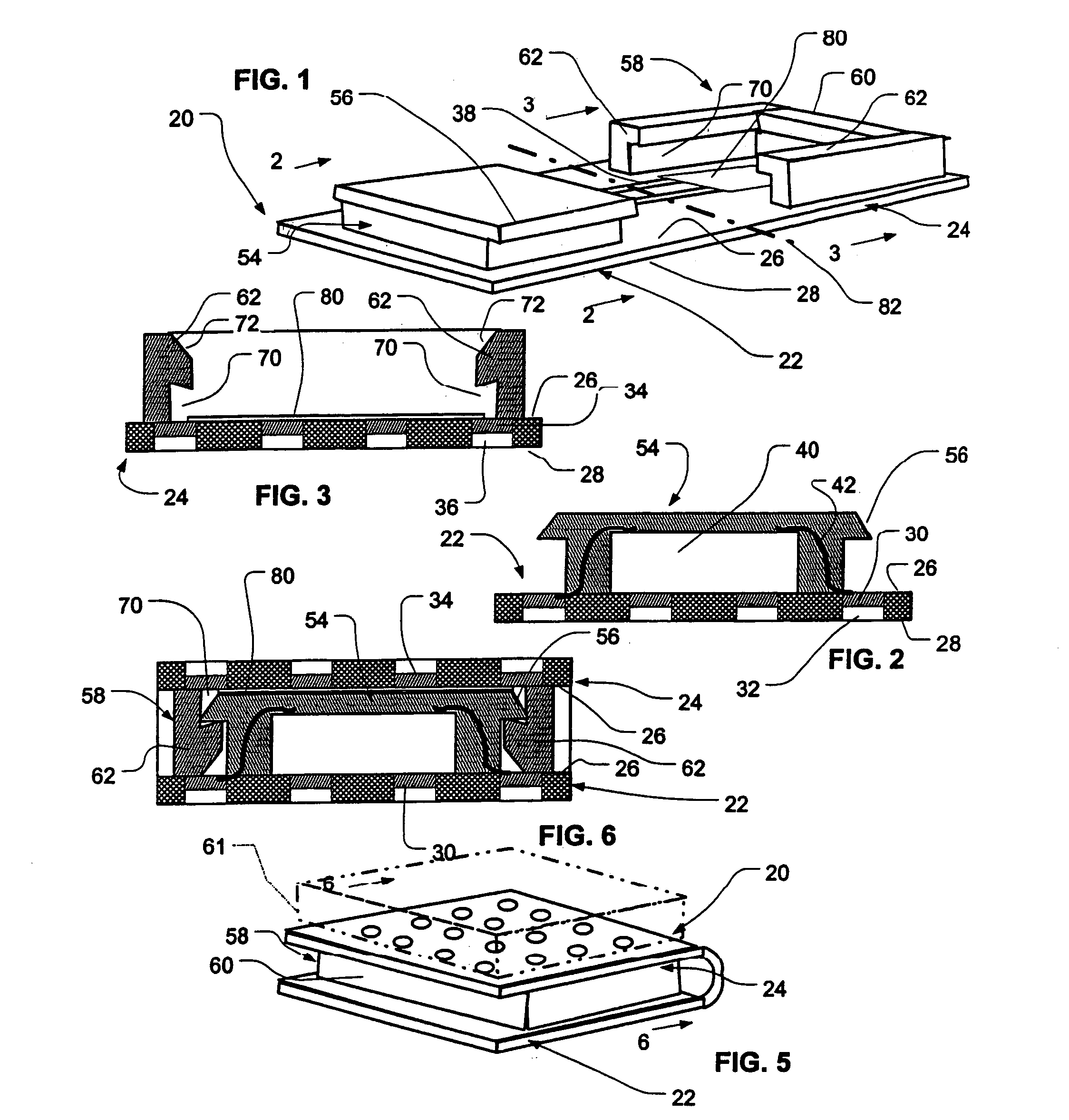
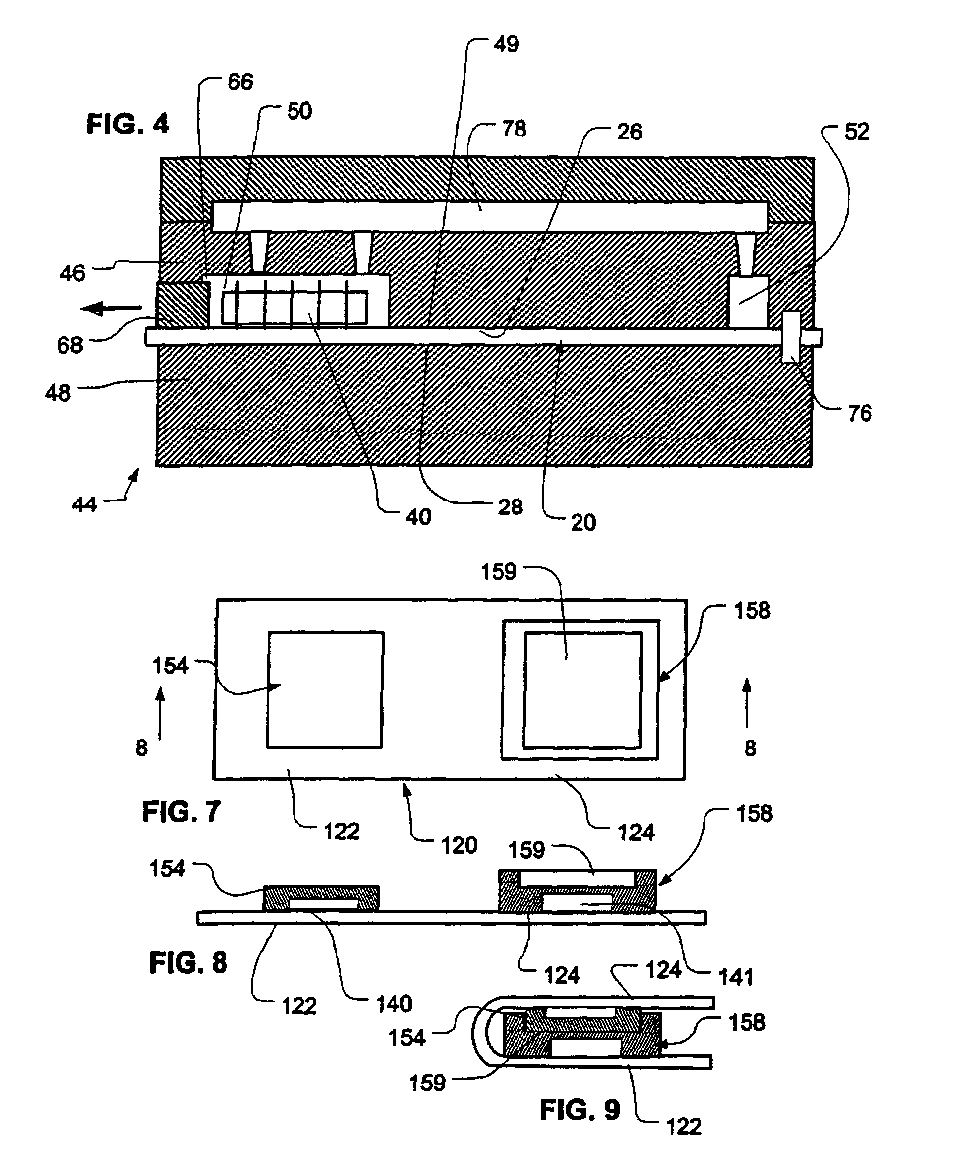
[0032]A component according to one embodiment of the invention includes a dielectric substrate 20 in the form of an elongated strip having a first part 22 adjacent one end and a second part 24 adjacent the opposite end. The substrate has an interior surface 26 (the surface facing upwardly in FIG. 1) and an exterior surface 28 (facing downwardly in FIG. 1). A set of electrically conductive mounting terminals 30 (FIG. 2) are provided on the first part 22 of the substrate. Terminals 30 are disposed at or near the interior surface 26 of the substrate and exposed to the exterior surface through holes or vias 32 extending through the substrate. Connecting terminals 34 (FIG. 3) are provided in the second part 24 of the substrate. The connecting terminals are exposed to the external surface 28 of the substrate through holes 36. The substrate also includes electrically conductive traces 38 extending between the first and second parts of the substrate and interconnecting at least some of the ...


PUM


Abstract

A microelectronic package is made by a process which includes folding a substrate. Alignment elements on different parts of the substrate engage one another during the folding process to position the parts of the substrate precisely relative to one another. One or more of the alignment elements may be a mass of an overmolding encapsulant covering a chip.

Description

CROSS-REFERENCE TO RELATED APPLICATIONS[0001]The present application claims benefit of U.S. Provisional Patent Application Ser. No. 60 / 403,939, filed Aug. 16, 2002, the disclosure of which is hereby incorporated by reference herein.FIELD OF THE INVENTION[0002]The present invention relates to microelectronic assemblies and to components and methods for making the same.BACKGROUND OF THE INVENTION[0003]Certain microelectronic packages are made using a sheet like element incorporating a dielectric layer structure and mounting terminals disposed on this structure. Some or all of the terminals are connected to the microelectronic device to be packaged. In many cases, the active microelectronic device such as a semiconductor chip is covered by an encapsulant. The encapsulant commonly is molded in place on the dielectric layer so that the mass of encapsulant has a preselected shape, and so that the encapsulant covers the microelectronic device. The encapsulant may also cover features such a...

Claims


Application Information

Patent Timeline
Patent Type & Authority Patents(United States)
IPC IPC(8): H01L23/04H01L23/34H01L23/544H05K1/00H01L23/31H01L23/498H01L25/10
CPCH01L23/3121H01L23/4985H01L23/544H01L25/105H01L2924/1815H01L2224/48472H01L2225/1058H01L2225/1041H01L2225/1023H01L2223/54473H01L2224/4824H01L2924/01078H01L2924/01079H01L2924/15311H01L2924/3011H01L24/48H01L2924/00H01L2224/05599H01L2224/45099H01L2224/85399H01L2924/00014H01L2924/181
Inventor BANG, KYONG-MOKANG, TECK-GYUPARK, JAE M.
Owner TESSERA INC
Why Eureka
Try Eureka