Method for producing a spiral inductance on a substrate, and a device fabricated according to such a method
a technology of spiral inductance and substrate, which is applied in the manufacture of inductances/transformers/magnets, transformers/inductance coils/windings/connections, etc., can solve the problems of substrate loss, performance loss in regard to resonance frequency and quality factor, and low quality factor relative low, so as to achieve simple and cost-effective method, reduce electrical losses, and simple grounding
- Summary
- Abstract
- Description
- Claims
- Application Information
AI Technical Summary
Benefits of technology
Problems solved by technology
Method used
Image
Examples
first embodiment
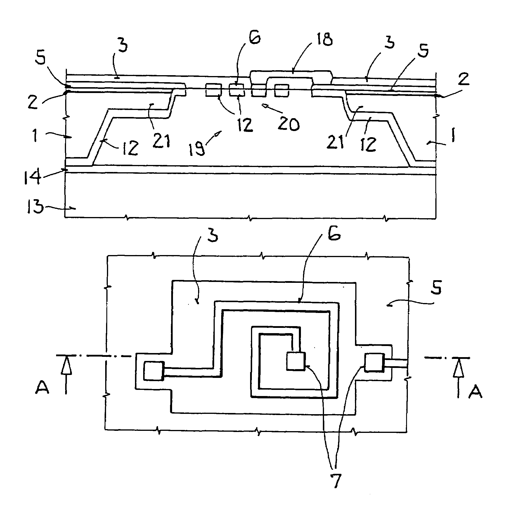
[0052]FIGS. 7a to 7m illustrate cross-sectional views of an exemplary device in selected method modes, whereby with reference to FIGS. 7a to 7m, a production method for a device having a spiral inductance on a substrate according to the present invention is described in detail.
[0053]As is shown in FIG. 7a, for example, in a step for the fabrication of metallizations, the top and bottom sides of a substrate 1 are coated with a first layer, for example, a first dielectric insulating layer 2, that is, a further dielectric insulating layer 4 (henceforth referred to as third insulating layer 4). However, in certain instances, layers 2 and 4 can also be omitted. The substrate 1 is, for example, a low-resistance silicon semiconductor substrate, or the like. Both the first and the third dielectric insulating layer 2, or 4, can be formed, for example, as an approximately 1–2 μm-thick silicon nitride or silicon dioxide layer. Subsequently, an inductance metallization 6 and an upper ground met...
fourth embodiment
[0081]FIG. 11 illustrates a cross-sectional view of a device according to the present invention. As is shown in FIG. 11, a covering metallization 16 is additionally formed over the spiral inductance, whereby the rim areas of the covering metallization 16 are respectively connected with the upper ground metallization. The covering metallization 16 can be deposited by using a thick additional photoresist layer on the top side of the instant device. After a structuring of the SU-8 membrane 3 (again, preferably done during the application of the SU-8 layer), a thick photoresist layer, for example, about 30 μm thick, is deposited on the second dielectric insulating layer 3, and structured. Preferably, the sharp corners of the additional photoresist material can be smoothened, for example, by using an oxygen-plasma etching procedure. Thereafter, the shape of the covering metallization can be formed as a shield from external soiling and interferences by applying a standard metallization pr...
PUM
| Property | Measurement | Unit |
|---|---|---|
| inductance | aaaaa | aaaaa |
| thick | aaaaa | aaaaa |
| spiral inductance | aaaaa | aaaaa |
Abstract
Description
Claims
Application Information


