Eureka AIR delivers breakthrough ideas for toughest innovation challenges, trusted by R&D personnel around the world.

Apparatus for random access memory array self-test

Inactive Publication Date: 2006-05-30
AVENPORE PROPERTIES LLC
View PDF3 Cites 6 Cited by
  • Summary
  • Abstract
  • Description
  • Claims
  • Application Information

AI Technical Summary

Benefits of technology

[0008]In one representative embodiment, an electronic circuit for self-test of a random access memory array is disclosed wherein the random access array has a plurality of memory storage cells, wherein the storage cells are organized into a plurality of slice arrays. The electronic circuit includes a control circuit, an address selection circuit, an input/output circuit associated with each slice array, and an error detection circuit. The control circuit directs the address selection circuit to index through memory addresses

Problems solved by technology

In the sense of containing a larger number of memory cells where each cell can store one bit, the larger a RAM becomes, the more difficult and expensive it is to test it.
Also, the more expensive the cost of a defect in the circuit, as a single defect can result in the loss of the whole chip.
With the size and complexity of modern integrated circuits including RAM's, testing has become an important issue.
Size and cost constraints limit the area on the integrated circuit available for use as wire bonding pads, flip-chip solder bumps, and the like with the resultant effect of limiting access to the various functioning areas of the chip.
So, not all functions of the chip are externally available for direct test.
Even if connections to some of these areas were available, the long traces and additional external circuitry necessary to access them would introduce signal delays that could render the results of such testing questionable.
On-chip testing also has its share of difficulties as chip area available for testing is limited, as is accessibility to nodes for testing.
Delays introduced by trace lengths also continue to be an issue.
In addition unless the chip is designed for mass production, the costs associated with design, manufacturing, and test can be prohibitive.
Once again, however, unless the chip is designed for mass production, design costs can be prohibitive.

Method used


Image

  • Apparatus for random access memory array self-test
  • Apparatus for random access memory array self-test
  • Apparatus for random access memory array self-test

Examples


Embodiment Construction

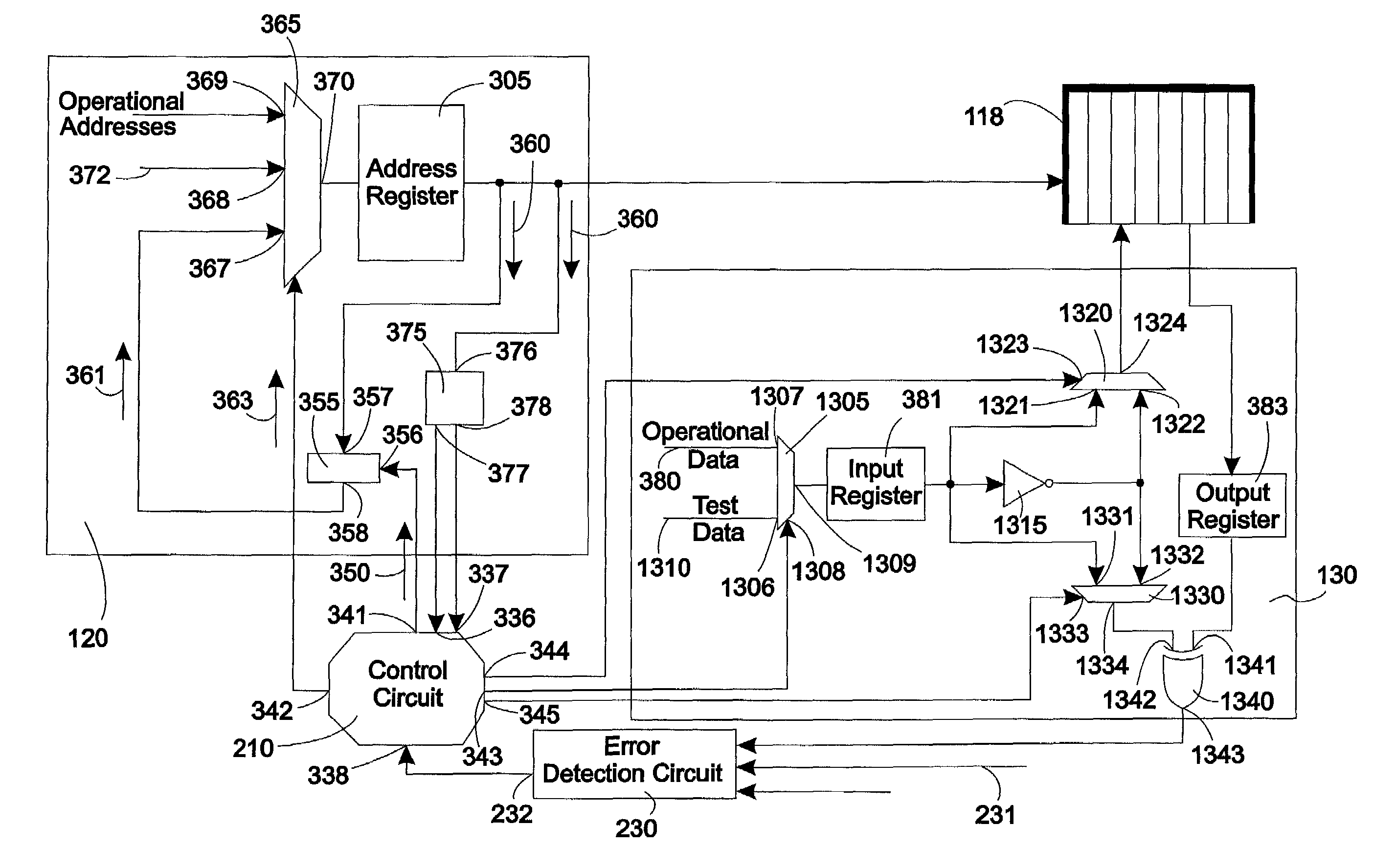
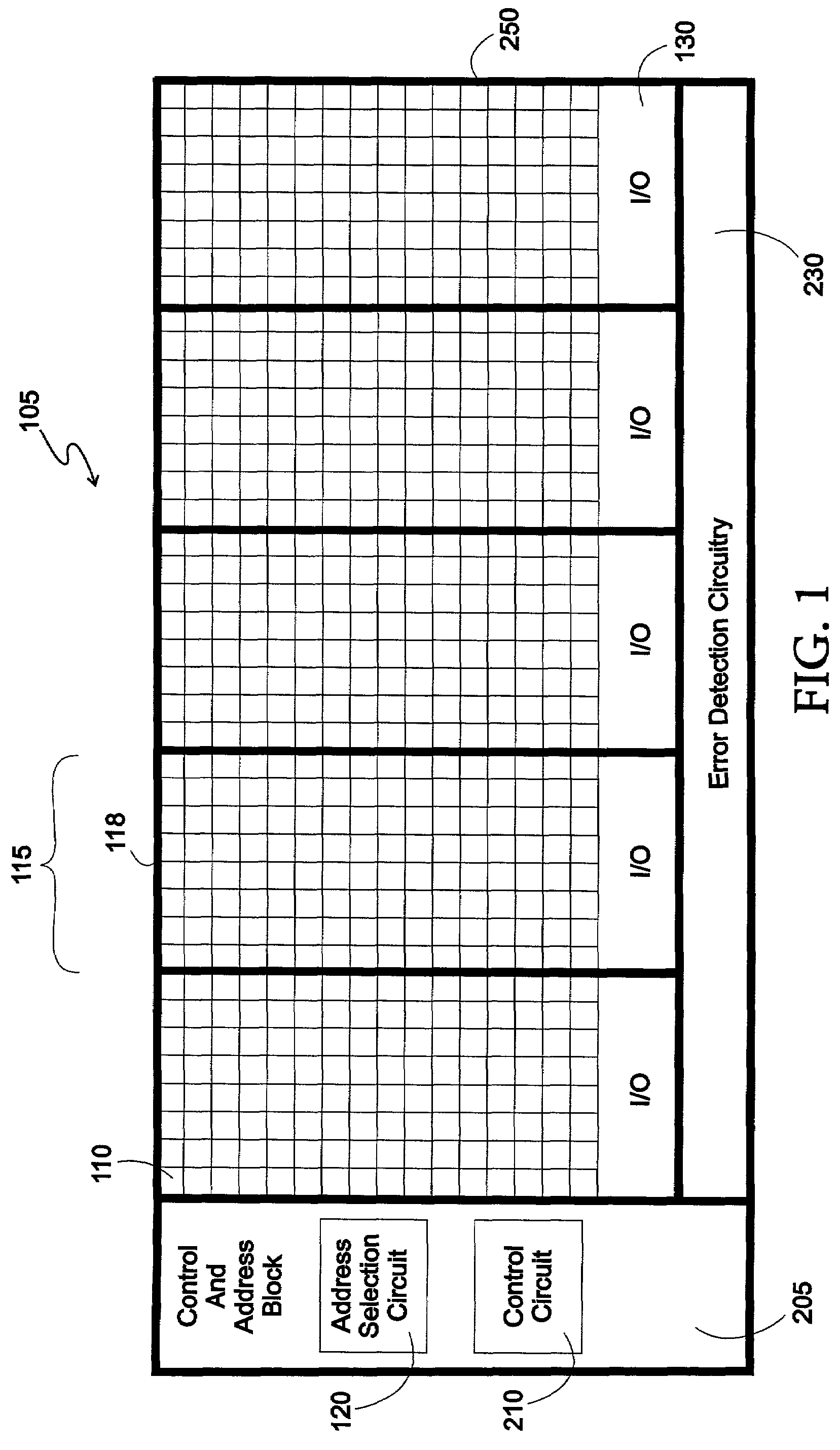
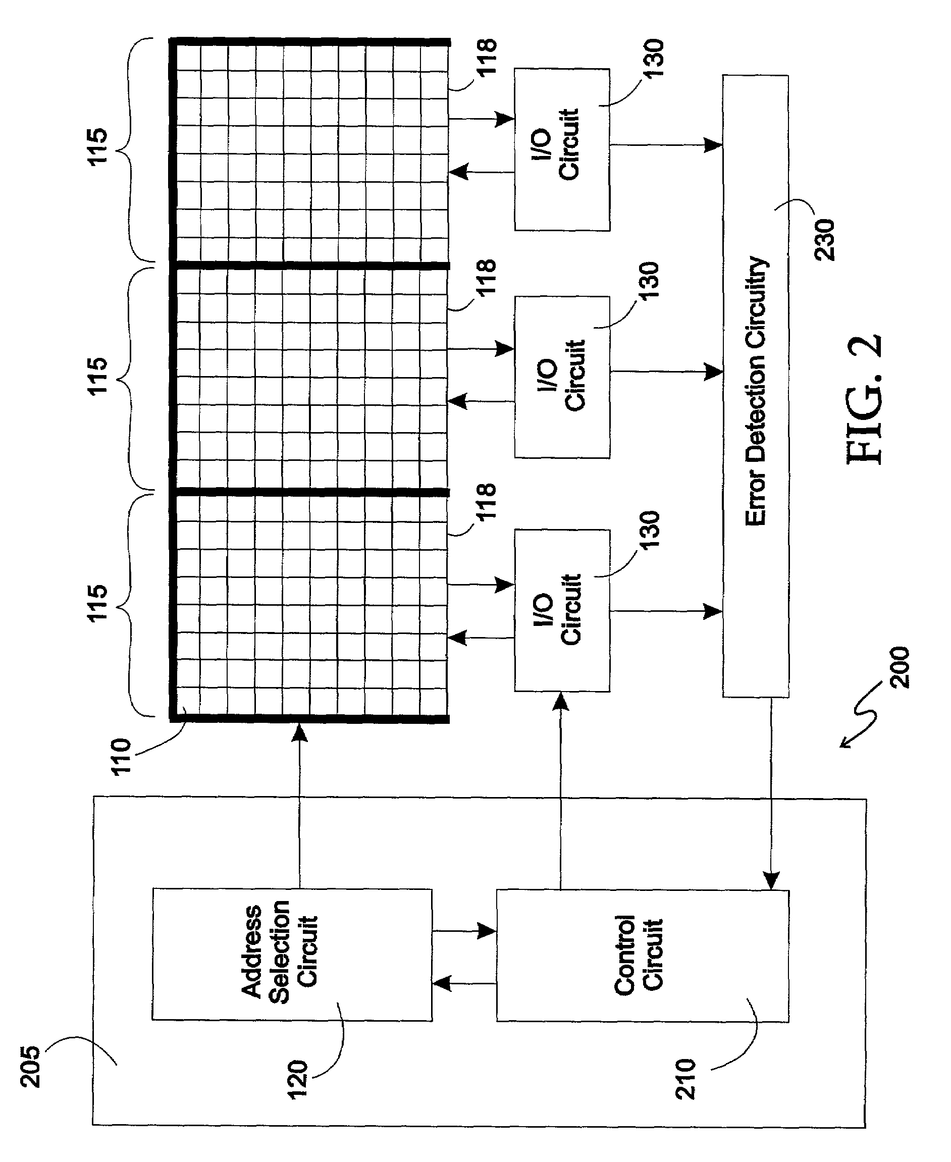
[0017]As shown in the drawings for purposes of illustration, the present patent document relates to novel apparatus for the automatic testing of RAM circuits on-chip. Previous circuitry for on-chip testing have required substantial area on the integrated circuit (IC) chip and have been somewhat removed from the tested area introducing propagation delay errors. By locating the circuitry necessary to perform such test in the addressing and input / output blocks of the RAM, these problems have been reduced.

[0018]Also, as shown in the drawings for purposes of illustration, the present patent document relates to novel apparatus for the repair of defective RAM circuits. Previous methods for repair of RAM circuits have typically used techniques such as laser repair which permit the removal of defective parts of the integrated circuit chip and then replacement with a redundant part. However, this process is expensive as an additional processing step is involved. By including the circuitry nec...


PUM


Abstract

An apparatus for the on-chip testing of random access memory arrays. In representative embodiments, embedded circuitry provides the ability to test random access memory arrays on-chip without requiring substantial area on the chip. The circuits are inherently located closer to the tested area which reduces propagation delay errors. These advantages have been obtained by locating the circuitry necessary to perform such test in the addressing and input / output blocks of the RAM.

Description

FIELD OF THE INVENTION[0001]The present invention relates generally to random access memories (RAM) in integrated circuits and, more particularly, to the test of such circuits and, even more particularly, to their test on-chip.BACKGROUND OF THE INVENTION[0002]Motivated by the desire for both lower cost and higher performance, integrated circuit (IC) technology has moved throughout its history toward building larger and larger circuits comprising more and more devices. The development of random access memory (RAM) integrated circuits have shared in this movement. In the sense of containing a larger number of memory cells where each cell can store one bit, the larger a RAM becomes, the more difficult and expensive it is to test it. Also, the more expensive the cost of a defect in the circuit, as a single defect can result in the loss of the whole chip.[0003]Not only are RAM's fabricated as stand-alone chips, but they are also built embedded as function blocks in other integrated circu...

Claims


Application Information

Patent Timeline
IPC IPC(8): G11C29/00G11C29/38
CPCG11C29/38G11C2029/1206
Inventor KOSS, LOUISE A.NASH, MARY LOUISEBEUCLER, DALE
Owner AVENPORE PROPERTIES LLC
Why Eureka
Eureka Blog
Learn More