Non-volatile semiconductor memory device and semiconductor memory device

a non-volatile, memory device technology, applied in static storage, digital storage, instruments, etc., can solve the problems of difficult to achieve high-speed operation, difficult to ensure accurate memory cell selection operation, and inability to correct errors, etc., to achieve accurate data reading and high speed

Inactive Publication Date: 2006-02-16
RENESAS ELECTRONICS CORP
View PDF1 Cites 81 Cited by
  • Summary
  • Abstract
  • Description
  • Claims
  • Application Information

AI Technical Summary

Benefits of technology

[0013] An object of the present invention is to provide a non-volatile ...

Problems solved by technology

Accordingly, a margin for the timing of starting memory cell selection becomes smaller, making it difficult to guarantee accurate memory cell selecting operation.
In order to ensure sufficient margin for the memory cell selecting operation and the data reading operation, it is necessary to set the timing of memory cell selection/data re...

Method used


Image

  • Non-volatile semiconductor memory device and semiconductor memory device
  • Non-volatile semiconductor memory device and semiconductor memory device
  • Non-volatile semiconductor memory device and semiconductor memory device

Examples


first embodiment

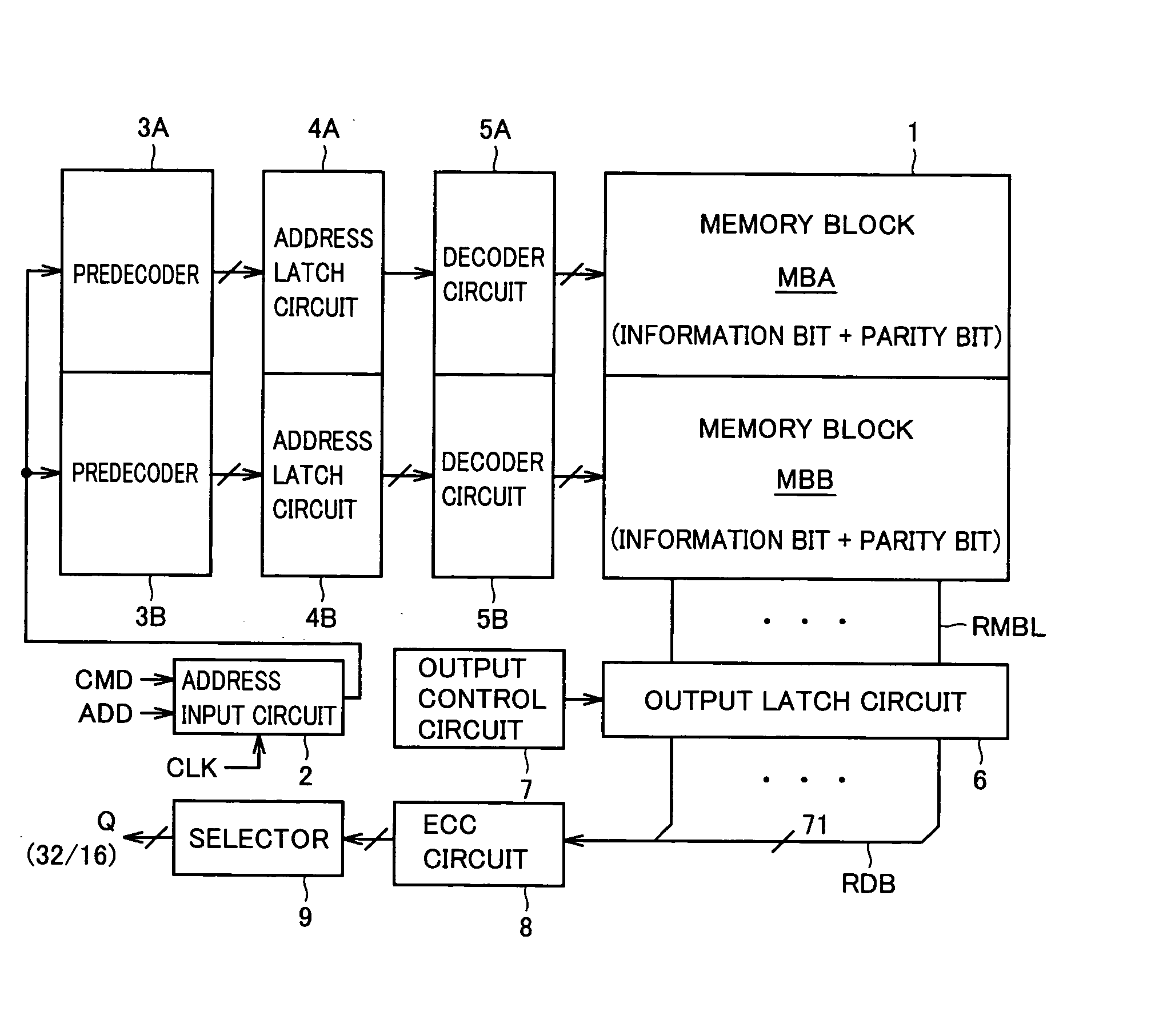
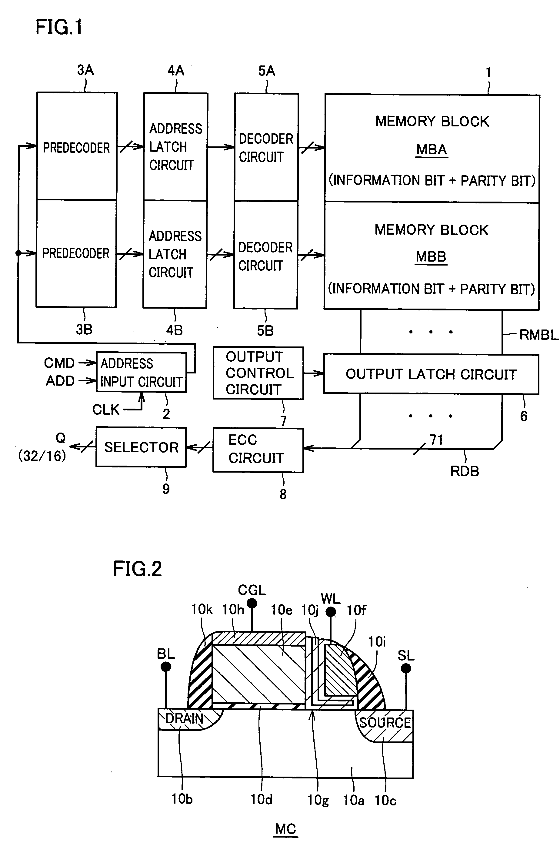
[0061]FIG. 1 schematically shows a construction of a main portion of a non-volatile semiconductor memory device in accordance with the first embodiment of the present invention.

[0062]FIG. 1 shows only the construction of the portion related to data reading, and constructions of portions related to data writing (programming) and erasure are not shown.

[0063] Referring to FIG. 1, the non-volatile semiconductor memory device includes a memory array 1 having non-volatile memory cells arranged in rows and columns. Memory array 1 is divided into two memory blocks MBA and MBB. Memory blocks MBA and MBB each store information (data) bits and parity bits for forming ECC codes for error detection / correction of the information bits. The parity bits are stored dispersed uniformly in each of the memory blocks MBA and MBB.

[0064] The non-volatile semiconductor memory device further includes: an address input circuit 2 taking an external command CMD and an address signal ADD in accordance with a ...

second embodiment

[0089]FIG. 5 more schematically shows the construction of memory array 1 and decode circuits 5a and 5b shown in FIG. 1. FIG. 5 shows a construction in one memory block of memory blocks MBA and MBB of memory array 1. Memory block MB (MBA or MBB) includes 8 memory mats MM0U-MM3U and MM0L-MM3L. Each of the memory mats MM0U-MM3U and MM0L-MM3L includes an information bit region IBR for storing information (data) bits and a parity region PBR for storing parity bits. In information bit region IBR, 16 bit line blocks each including 32 bit lines (subbit lines) are provided, and a total of 512 bit lines (subbit lines) are arranged.

[0090] Decode circuit 5 (5A or 5B) includes an X decoder 12u provided corresponding to memory mats MM0U-MM3U arranged in alignment in a row extending direction, an X decoder 12l provided corresponding to memory mats MM0L-MM3L arranged in the row extending direction, and a Y decoder 13. X decoders 12u and 12l decode a latched address (predecode address signal) from ...

third embodiment

[0105]FIG. 7 schematically shows a construction of a portion for reading 1 bit of internal data, of the non-volatile semiconductor memory device according to the third embodiment of the present invention. In FIG. 7, a construction of a portion for reading 1 bit of memory cell data from memory mats MMk and MMj is shown as a representative. Memory mats MMk and MMj correspond to the memory mat MMU (MM0U-MM3U) and MML (MM0L-MM3L) shown in FIG. 5.

[0106] In each of memory mats MMk and MMj, one bit line (subbit line) is selected from 32 bit lines (subbit lines) SBL. Here, 32 subbit lines are divided into subbit line groups BLG0-BLG3 each including 8 subbit lines SBL. A memory cell is connected to a subbit line SBL. Here, in an internal data reading path, the data is successively transmitted through the common bit line to the main bit line, and therefore, the bit line to which the memory cell is connected will be referred to as the subbit line.

[0107] In memory mat MMk, there are provided ...


PUM


Abstract

For each memory block, a predecoder for predecoding an applied address signal, an address latch circuit for latching the output signal of the predecoder, and a decode circuit for decoding an output signal of the address latch circuit and performing a memory cell selecting operation in a corresponding memory block are provided. Propagation delay of latch predecode signals can be made smaller and the margin for the internal read timing can be enlarged. In addition, the internal state of the decoder and memory cell selection circuitry are rest to an initial state when a memory cell is selected and the internal data output circuitry is reset to an initial state in accordance with a state of internal data reading. Thus, a non-volatile semiconductor memory device that can decrease address skew and realize an operation with sufficient margin is provided.

Description

BACKGROUND OF THE INVENTION [0001] 1. Field of the Invention [0002] The present invention relates to a semiconductor memory device and a construction of a portion related to data reading for reading data accurately at high speed. Specifically, the present invention relates to a construction for achieving high-speed data reading in a non-volatile semiconductor memory device. [0003] 2. Description of Background Art [0004] A non-volatile semiconductor memory device such as a flash memory is widely used in the field of portable equipments and the like as it can store data in a non-volatile manner. A memory cell structure of the non-volatile semiconductor memory device is roughly divided into a structure utilizing a stacked gate type transistor in which charges are stored in a conductive floating gate formed of polysilicon or the like, and insulating film trap type memory cell structure in which charges are stored in an insulation film such as a nitride film. In either memory cell struct...

Claims


Application Information

Patent Timeline
IPC IPC(8): G11C8/00
CPCG11C8/10G11C16/32G11C16/28G11C16/08
Inventor OOISHI, TSUKASAUCHIYAMA, TOMOHIROMIYAZAKI, SHINYA
Owner RENESAS ELECTRONICS CORP
Why Eureka
Try Eureka