High density semiconductor memory device and method for manufacturing the same

a high-density semiconductor and memory device technology, applied in the direction of semiconductor devices, electrical appliances, nanotechnology, etc., can solve the problems of data storage time, data difficulty, data precision reading, etc., and achieve the effect of high density

Inactive Publication Date: 2013-03-28
ELECTRONICS & TELECOMM RES INST
View PDF5 Cites 0 Cited by
  • Summary
  • Abstract
  • Description
  • Claims
  • Application Information

AI Technical Summary

Benefits of technology

[0012]An embodiment of the present invention is directed to providing a high density semiconductor device capable of precisely reading data by suppressing the occurrence of a leakage current due to the high-integration of the semiconductor memory device, and a method for manufacturing the high density semiconductor memory device.
[0013]Another embodiment of the present invention is directed to providing a high density semiconductor device capable of simplifying a manufacturing process of the high density semiconductor device, and a method for manufacturing the high density semiconductor memory device.

Problems solved by technology

In particular, it is difficult to precisely read data because a threshold voltage of a transistor changes due to a leakage current caused by the SCE.
Therefore, in order to secure a sufficient space, i.e., a number of trap sites, for storing data, the floating gate 130 must have a great thickness, which makes it difficult to realize a high density flash memory.
In addition, since a trap force is weak when trapping charges into trap sites, there is a problem in that a data-storing time, i.e., a retention time is reduced.
Furthermore, in the conventional flash memory device, charges are injected or removed into / from the floating gate 130 using hot electron injection or Fowler-Nordheim (F-N) tunneling requiring a high voltage, for example, a voltage in the range of approximately 14 V to approximately 20 V, resulting in high power consumption.
Accordingly, the conventional flash memory device is disadvantageous in that the tunneling dielectric layer 120 is deteriorated due to a stress applied thereto while injecting or removing charges into / from the floating gate 130 and further data stored in the floating gate 130 may be lost due to charge leakage.

Method used


Image

  • High density semiconductor memory device and method for manufacturing the same
  • High density semiconductor memory device and method for manufacturing the same
  • High density semiconductor memory device and method for manufacturing the same

Examples


Embodiment Construction

[0026]The advantages, features and aspects of the invention will become apparent from the following description of the embodiments with reference to the accompanying drawings, which is set forth hereinafter.

[0027]In the drawings, the dimensions of layers and regions are exaggerated for clarity of illustration. It will also be understood that when a layer (or film) is referred to as being ‘on’ another layer or substrate, it can be directly on the other layer or substrate, or intervening layers may also be present. Like reference numerals refer to like elements throughout the drawings.

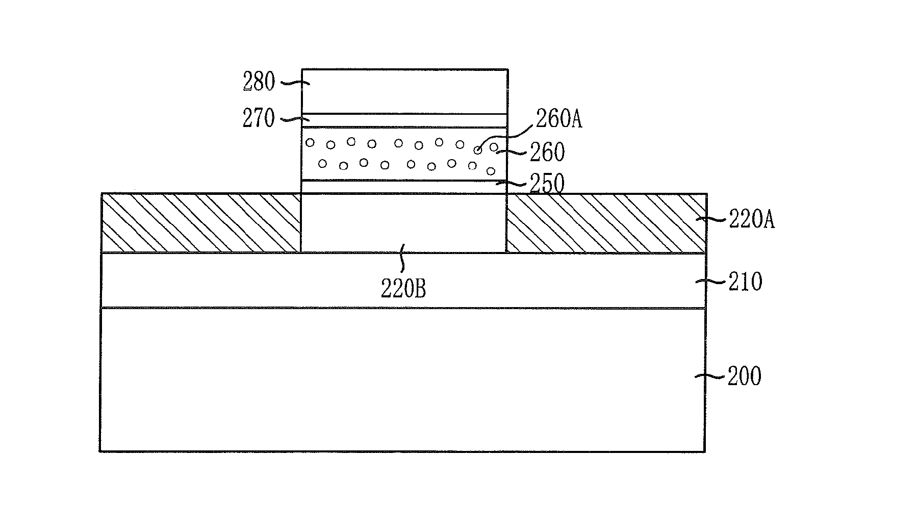
[0028]FIG. 2 is a cross-sectional view of a high density semiconductor memory device in accordance with an embodiment of the present invention.

[0029]Referring to FIG. 2, the high density semiconductor memory device of the present invention includes source and drain electrodes 220A and a floating gate 260A. The source and drain electrodes 220A are provided in a substrate and forms a Schottky junction with...


PUM


Abstract

Provided are a high density semiconductor memory device capable of precisely reading data by suppressing the occurrence of a leakage current due to the high-integration of the semiconductor memory device, and a method for manufacturing the semiconductor memory device. The high density semiconductor memory device includes: source and drain electrodes disposed over a substrate, and forming a Schottky junction with a channel region; and a floating gate disposed over the substrate of the channel region, and configured with a plurality of nanodots. The nanodots may be formed of a silicon compound or any material that can be charged.

Description

CROSS-REFERENCE(S) TO RELATED APPLICATIONS[0001]The present invention claims priority of Korean Patent Application Nos. 10-2006-0121224 and 10-2007-0094687, filed on Dec. 4, 2006, and Sep. 18, 2007, respectively, which are incorporated herein by reference.BACKGROUND OF THE INVENTION[0002]1. Field of the Invention[0003]The present invention relates to a semiconductor memory device and a method for manufacturing the same; and, more particularly, to a high density semiconductor memory device capable of precisely reading data by suppressing the occurrence of a leakage current due to the high-integration of the semiconductor memory device, and a method for manufacturing the semiconductor memory device.[0004]This work was supported by the IT R&D program of MIC / IITA.[0005]2. Description of Related Art[0006]Demands for flash memories among a variety of semiconductor memory devices have explosively increased for past several years with the advent of mobile devices such as mobile phones, came...

Claims


Application Information

Patent Timeline
Patent Type & Authority Applications(United States)
IPC IPC(8): H01L29/788H01L29/66
CPCB82Y10/00H01L21/28273H01L29/41725H01L29/42324H01L29/788H01L29/7839H01L29/78654H01L29/7881H01L29/66825H01L29/47H01L29/40114
Inventor KIM, TAEYOUBJUN, MYUNGSIMKIM, YARK-YEONJANG, MOON-GYUCHOI, CHEL-JONGLEEPARK, BYOUNGCHUL
Owner ELECTRONICS & TELECOMM RES INST
Why Eureka
Try Eureka