Antenna on a wireless untethered device such as a chip or printed circuit board for harvesting energy from space

a wireless untethered device and antenna technology, applied in the direction of burglar alarm mechanical actuation, burglar alarm by hand-held items removal, etc., can solve the problems of limiting the ability to reduce the size of the antenna, the antenna location interferes with the layout of the conventional bond pad about the periphery of the chip, and the complexity and cost of the antenna on the chip. achieve the effect of facilitating efficient energy receipt, enhancing the effective antenna area, and maximizing performan

Active Publication Date: 2006-06-06
UNIVERSITY OF PITTSBURGH
View PDF12 Cites 50 Cited by
  • Summary
  • Abstract
  • Description
  • Claims
  • Application Information

AI Technical Summary

Benefits of technology

[0016]The antenna may be a spiral antenna such as a square spiral antenna, with the thickness and width of the conductive portion being adjusted to maximize performance. Impedance may be adjusted to provide for an enhanced effective antenna area.
[0017]It is an object of the present invention to provide an integrated antenna on a chip or printed circuit board with associating circuitry to facilitate efficient receipt of energy from space by the antenna and conversion of the same by the circuitry to DC power.

Problems solved by technology

One of the problems with the approach as taught in U.S. Pat. Nos. 4,857,893 and 4,724,427 is the need to fabricate small, air core inductors of sufficiently high inductance and Q for integrated circuit applications.
Such an approach increases the complexity and cost of the antenna on a chip and also limits the ability to reduce the size of the antenna because of the need for the magnetic film layers between the antenna coils.
Another problem with the approach as taught in U.S. Pat. Nos. 4,857,893 and 4,724,427 is the attendant integrating of an antenna on an integrated circuit (IC) chip.
In the case of an antenna disposed about the periphery of the chip, as described by the patents discussed hereinabove, the location of the antenna interferes with conventional bond pad layout about the periphery of the chip.
Also, the electromagnetic fields within the central area of an antenna laid out about the periphery of a chip can interfere with the operation of circuits located within the antenna.
A problem with the prior art as discussed above is that disposition of the antenna on the chip is limited to specific different parts of the chip.
A further problem with the antenna on chip designs as disclosed by prior art is that the antenna and IC circuitry are disposed as discrete components in separate portions of the chip to minimize the interaction of the antenna and the circuitry of the IC chip.
This again limits the design of placing an antenna on a IC chip.
Furthermore, it makes for devices that are not truly integrated.

Method used


Image

  • Antenna on a wireless untethered device such as a chip or printed circuit board for harvesting energy from space
  • Antenna on a wireless untethered device such as a chip or printed circuit board for harvesting energy from space
  • Antenna on a wireless untethered device such as a chip or printed circuit board for harvesting energy from space

Examples


Embodiment Construction

[0051]As employed herein, the tern “in space” means that energy or signals are being transmitted through the air or similar medium regardless of whether the transmission is within or partially within an enclosure, as contrasted with transmission of electrical energy by a hard wired or printed circuit boards.

[0052]As employed herein the term “wireless untethered device” means a device which is remotely powered by RF energy and shall include, but not be limited to, IC chips, printed circuit boards and other suitable substrates having discrete or integrated circuit components.

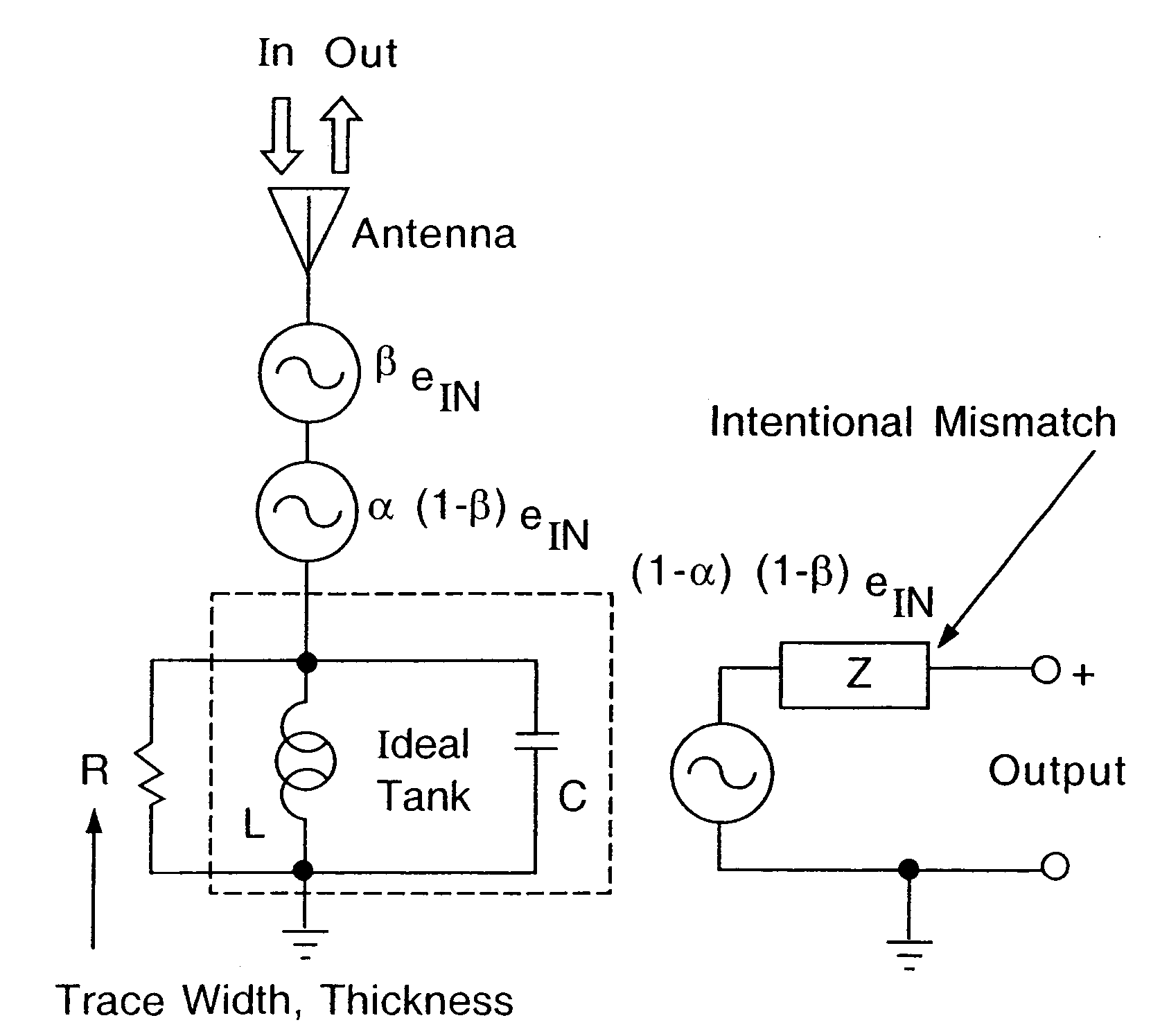
[0053]What is further needed is an antenna on a chip wherein the antenna is not a discrete component to the IC circuit. In that respect there are two issues; (1) the interference of the received RF energy on the proximate IC circuitry, and (2) the interference of the proximate IC circuitry on the RF energy. While the first issue is important to any functional IC, the separation of the energy harvesting function fr...


PUM


Abstract

A wireless untethered device which may be an integrated circuit chip or printed circuit board having at least one integrated antenna and circuitry operatively associated with the antenna for receipt of energy harvested from space by the antenna. The antenna has an effective area greater than its physical area. A system which receives power from the harvested energy after the energy is processed by the circuitry may also be provided with mismatched impedance between the antenna and a circuit resistance.

Description

CROSS-REFERENCE[0001]This application claims the benefit of U.S. Provisional Application Ser. No. 60 / 475,151 entitled “ANTENNA ON A WIRELESS UNTETHERED DEVICE SUCH AS A CHIP OR PRINTED CIRCUIT BOARD FOR HARVESTING ENERGY FROM SPACE” filed Jun. 2, 2003.BACKGROUND OF THE INVENTION[0002]1. Field of the Invention[0003]A device is disclosed comprising a semiconductor integrated circuit (IC) chip having disposed on it antenna and the circuitry for the IC chip, wherein antenna and the circuitry of the IC chip are integrated so as to provide the IC chip with an improved antenna effective area. The design of the antenna placement on the chip is independent of the location of the antenna on the chip. As a result, antenna-on-a-chips of this invention are simpler to design and manufacture than the designs disclosed in the prior art. With increasing dependence on local and wide area wireless networks, particularly those with low power (range) requirements and local sensing or object identificati...

Claims


Application Information

Patent Timeline
Patent Type & Authority Patents(United States)
IPC IPC(8): G08B13/14G06K19/07H01LH01Q1/22H01Q7/00H01Q23/00
CPCG06K19/0723H01Q1/22H01Q23/00H01Q1/2283H01Q7/00H01Q1/2225
Inventor MICKLE, MARLIN H.CAPELLI, CHRISTOPHER C.SWIFT, HAROLD
Owner UNIVERSITY OF PITTSBURGH
Why Eureka
Try Eureka