


Quick Research
Generate reliable direction feasibility study reports for your R&D in just a few steps.

Technical Q&A
Discover and master advanced knowledge NOW. Basics, ideas, possibilities, all at once.

Find Solutions
As an expert in R&D theories, this can generate solutions to your technical problems instantly.

Evaluate Feasibility
Analyze your overall solution with one click, know your potential R&D risks in advance.

Monitor Landscape
Get weekly tech updates, stay abreast of the latest tech innovations and key insights.
Optical detection device and optical device
a detection device and optical technology, applied in the direction of optical elements, line-of-sight transmission, instruments, etc., can solve the problems of inability to deal and reduce the intensity of the received light detected by the light receiving elemen
- Summary
- Abstract
- Description
- Claims
- Application Information
AI Technical Summary
Benefits of technology
Problems solved by technology
Method used
Image

Examples
example 1
[0067]Numerical limitations for a case in which a fresnel reflecting surface is used for an optical element are shown in FIG. 5. Reference numeral 31 indicates an aperture diaphragm.
[0068]
Surface No.rdDecentralization1Aperture Surfaced1 = 0.002Fresnel ReflectingD2 = 0.00Decentralizationsurface [r1](1)3∞(Image Surface)Decentralization[r2](2)Fresnel Reflecting surface [r1]Curvature−16.62K−1.3797a −3.7354 ×b 5.186 × 10⁻⁷c −1.0439 × 10⁻⁸d 5.7655 × 10−1110−5Decentralization (1)X0.00Y−5.01Z5.18α17.00β10.00γ10.00Decentralization (2)X0.00Y−7.00Z−2.5α285.00β20.00γ20.00
[0069]In such a case, it is possible to form a flat optical element. Therefore, it is possible to form a small, light-weight device. Thus, a mass-production is possible such that the cost can be reduced.
example 2
[0070]Numerical limitations for a case in which a refracting reflecting surface surface is used for an optical element are shown in FIG. 6. Reference numeral 32 indicates an aperture diaphragm.
[0071]
SurfaceNo.rDDecentralizationndνd1ApertureD3 =Surface20.00RefractiveReflecting2SurfaceD4 = 0.001001.068−3.5(F F S) [r3]3∞(ImageDecentralizationSurface)(1)[r2]F F S [r1]C3 −3.7924 × 10⁻⁴C4 −4.1412 × 10⁻⁶C6 −3.8132 × 10⁻⁶C8 9.1325 × 10⁻⁹C10 7.9132 × 10⁻¹⁰C11 1.4989 × 10⁻¹⁰C13 3.2546 × 10⁻⁹C15 −4.8971 × 10⁻¹¹Decentralization (1)X0.00Y−18.00Z3.00α3 90.00β30.00Γ30.00
[0072]In such a case, it is also possible to form a small, light-weight device similarly to a case in which a fresnel reflecting surface is used. Furthermore, it is not necessary to decentralize nor slant the optical surface; therefore, it is possible to form the device more compactly.
[0073]Here, in the above embodiments, it is possible to use the optical detection device and the optical system so as to detect the inclination of th...
third embodiment
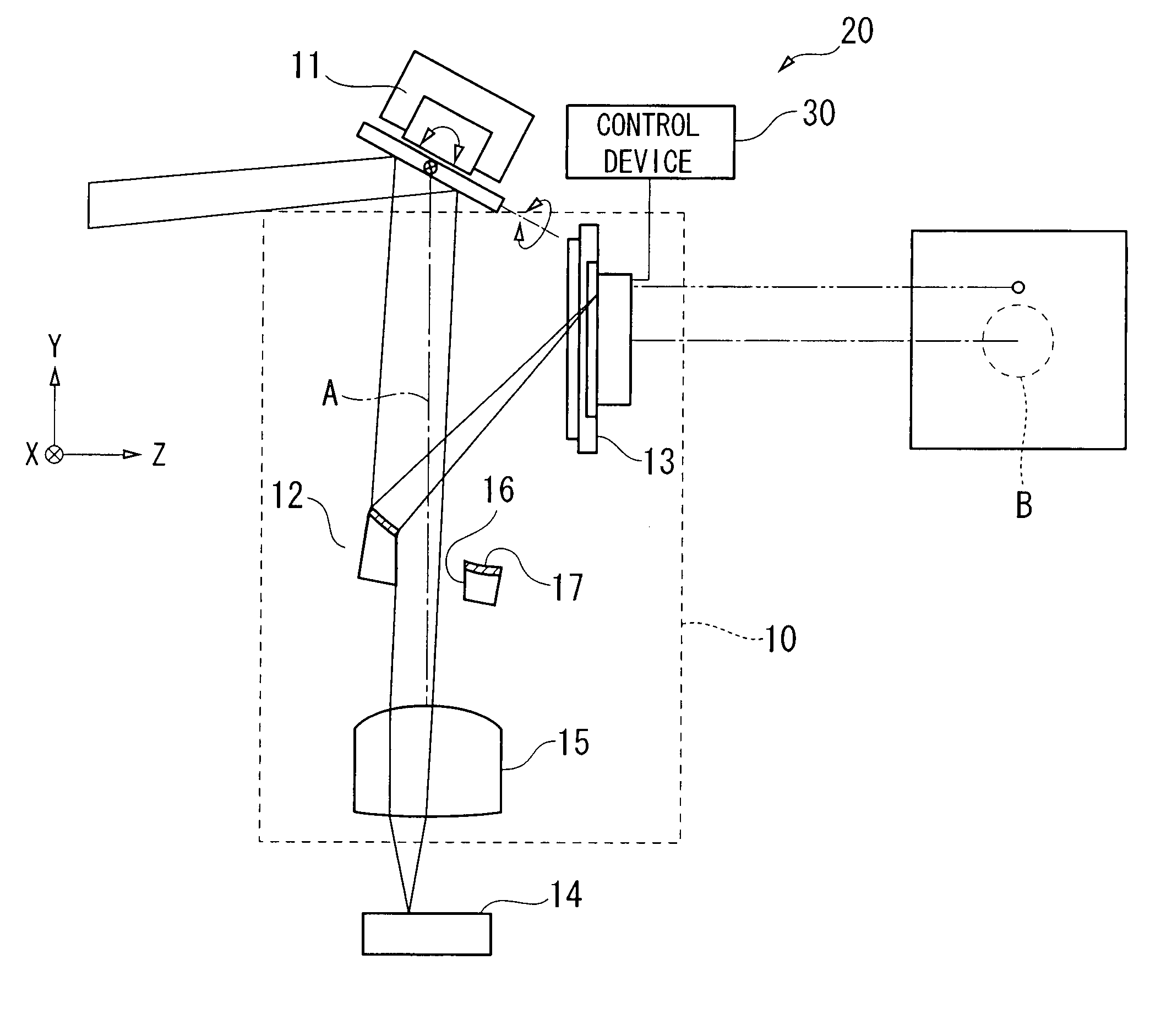
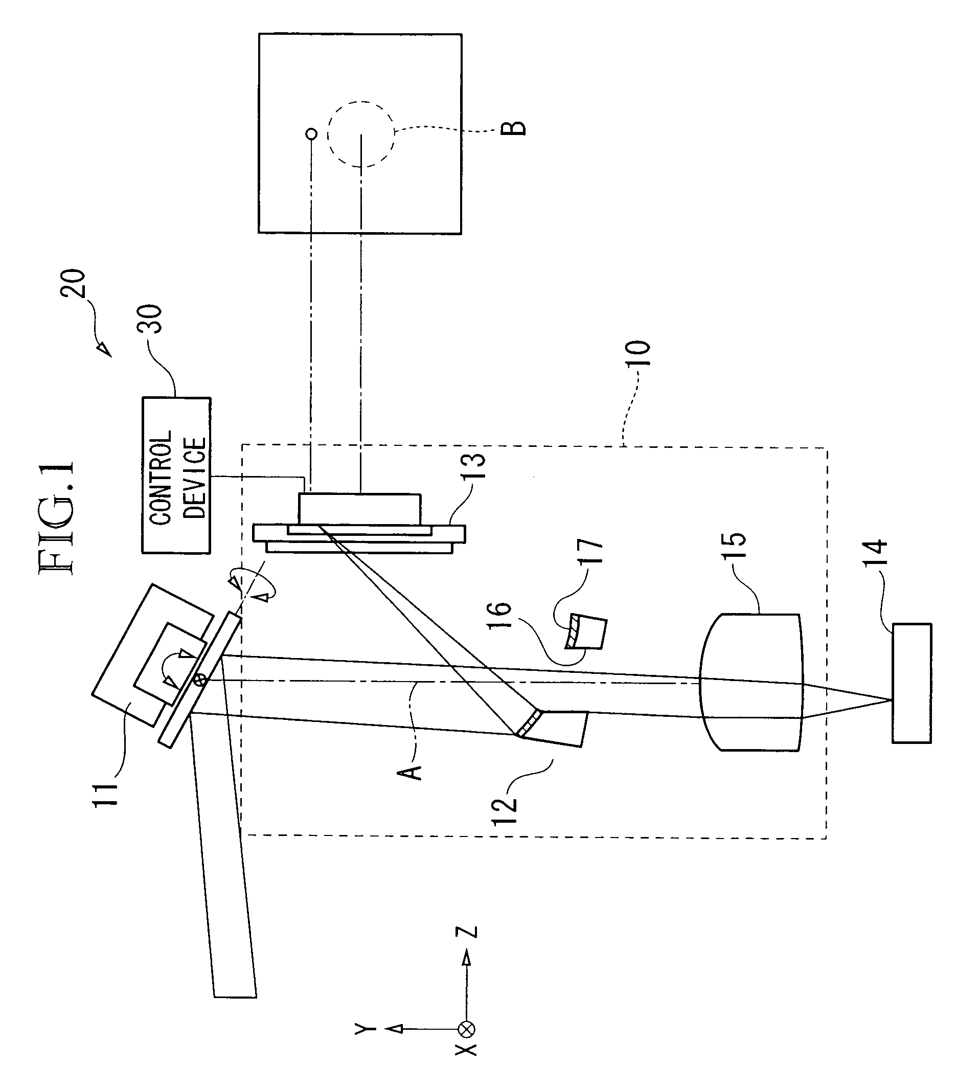
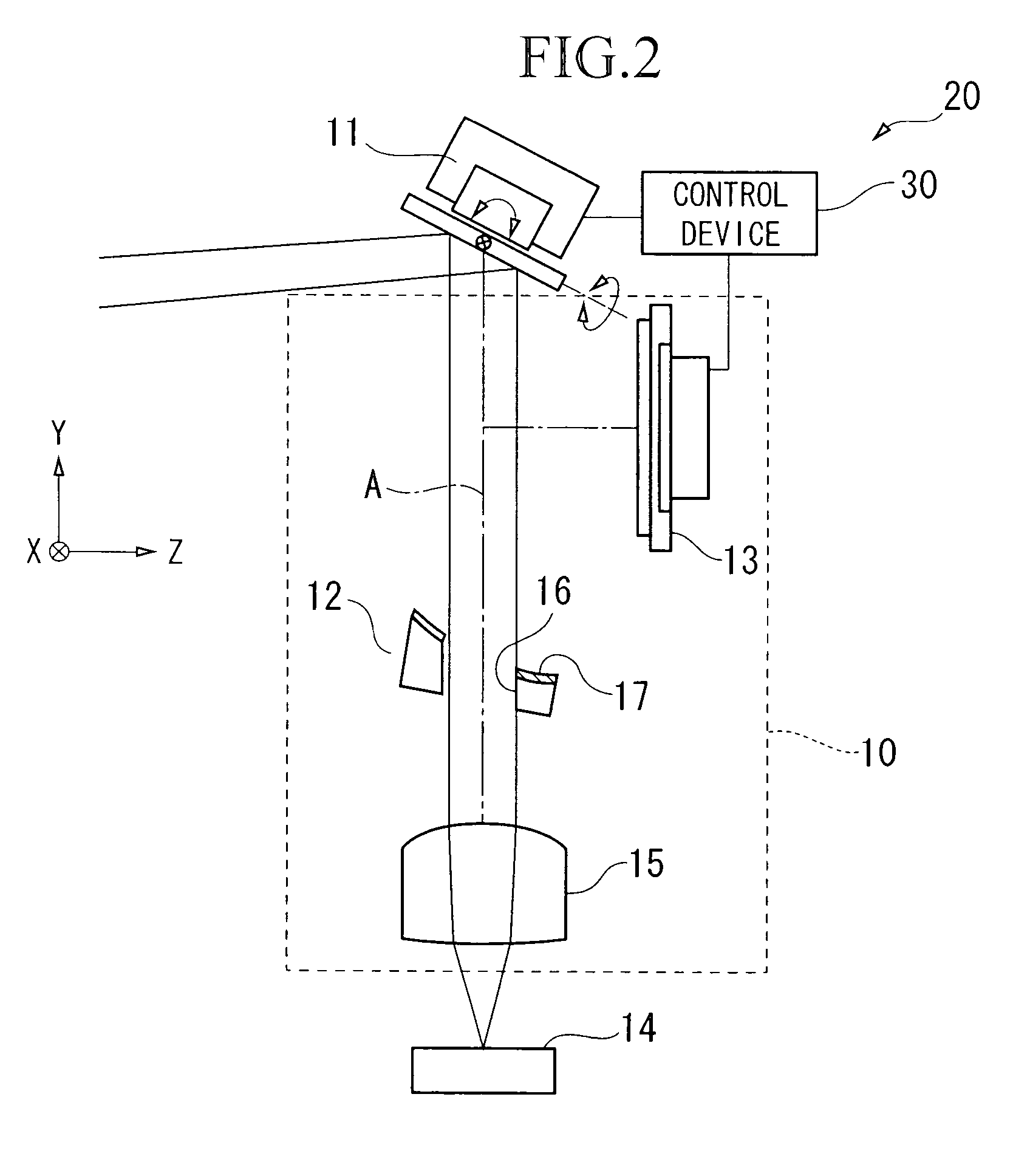
[0074]An optical tuning and tracking device according to a third embodiment of the present invention is explained. An optical capturing and tracking device according to the present embodiment comprises an optical device section and a light transmitting device section.
[0075]FIG. 8 is a cross section for explaining a general structure for an example of the optical capturing and tracking device according to the third embodiment of the present invention.
[0076]An optical tracking device 200 (optical capturing and tracking device) according to a third embodiment of the present invention is explained. The optical tracking device 200 serves for transmitting and receiving the light such that an approximate parallel incident light can be tracked. In particular, the optical tracking device 200 can be preferably used in the aerial optical communication field.
[0077]First, a light receiving device section in the optical tracking device 200 is explained.
[0078]In a general structure, the light rece...
PUM
 Abstract
Description
Claims
Application Information
 - R&D Engineer
- R&D Manager
- IP Professional
- Industry Leading Data Capabilities
- Powerful AI technology
- Patent DNA Extraction
Browse by: Latest US Patents, China's latest patents, Technical Efficacy Thesaurus, Application Domain, Technology Topic, Popular Technical Reports.
© 2024 PatSnap. All rights reserved.Legal|Privacy policy|Modern Slavery Act Transparency Statement|Sitemap|About US| Contact US: help@patsnap.com