

Semiconductor device having led out conductor layers, manufacturing method of the same, and semiconductor module
- Summary
- Abstract
- Description
- Claims
- Application Information
AI Technical Summary
Benefits of technology
Problems solved by technology
Method used
Image

Examples
Embodiment Construction
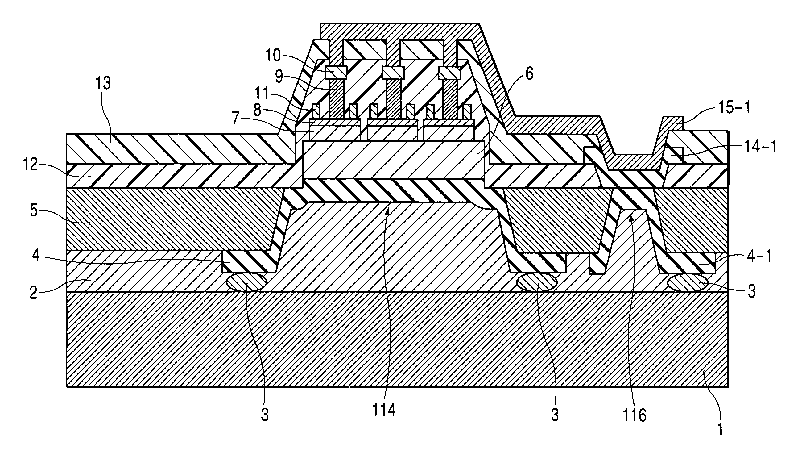
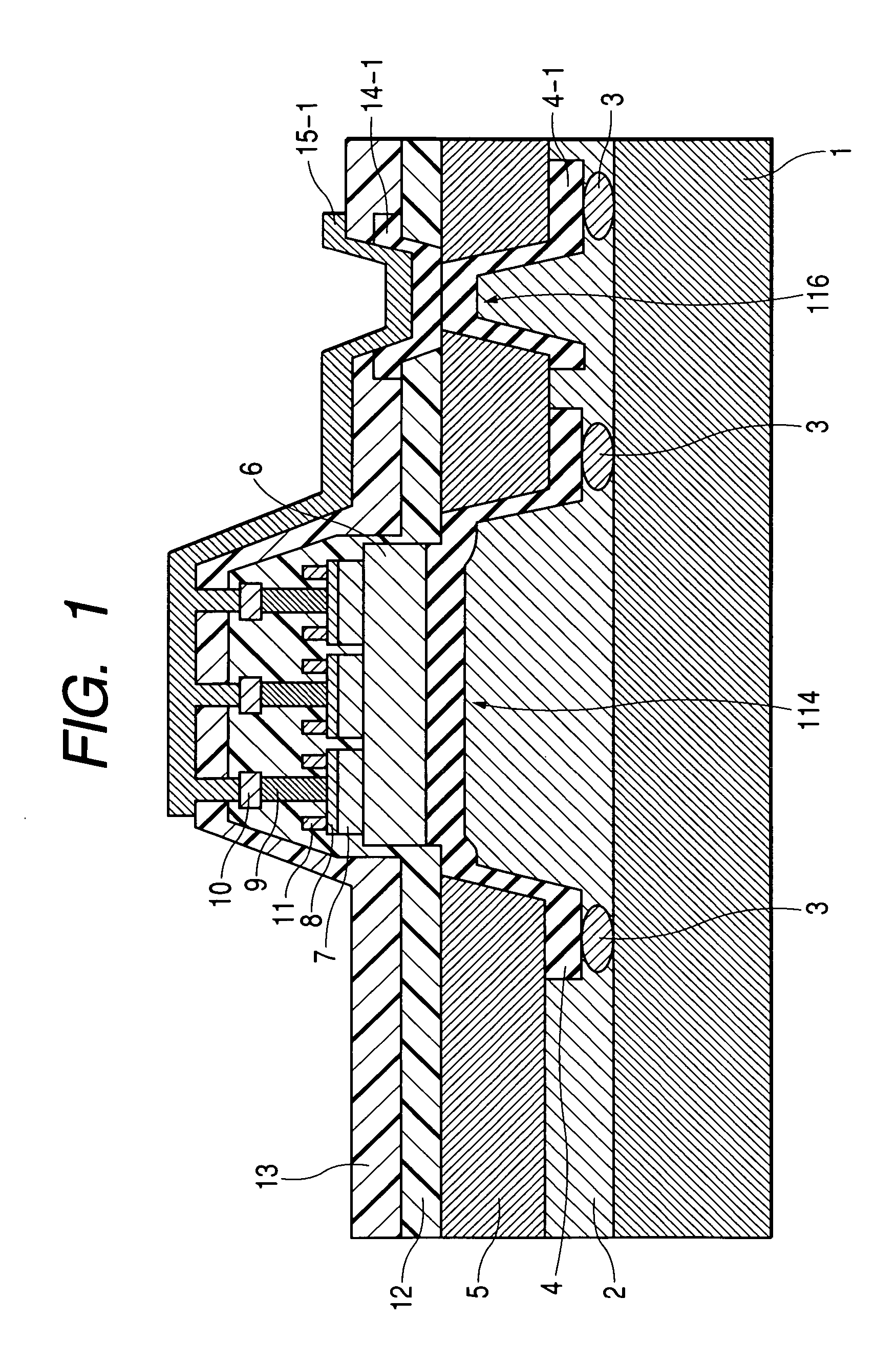
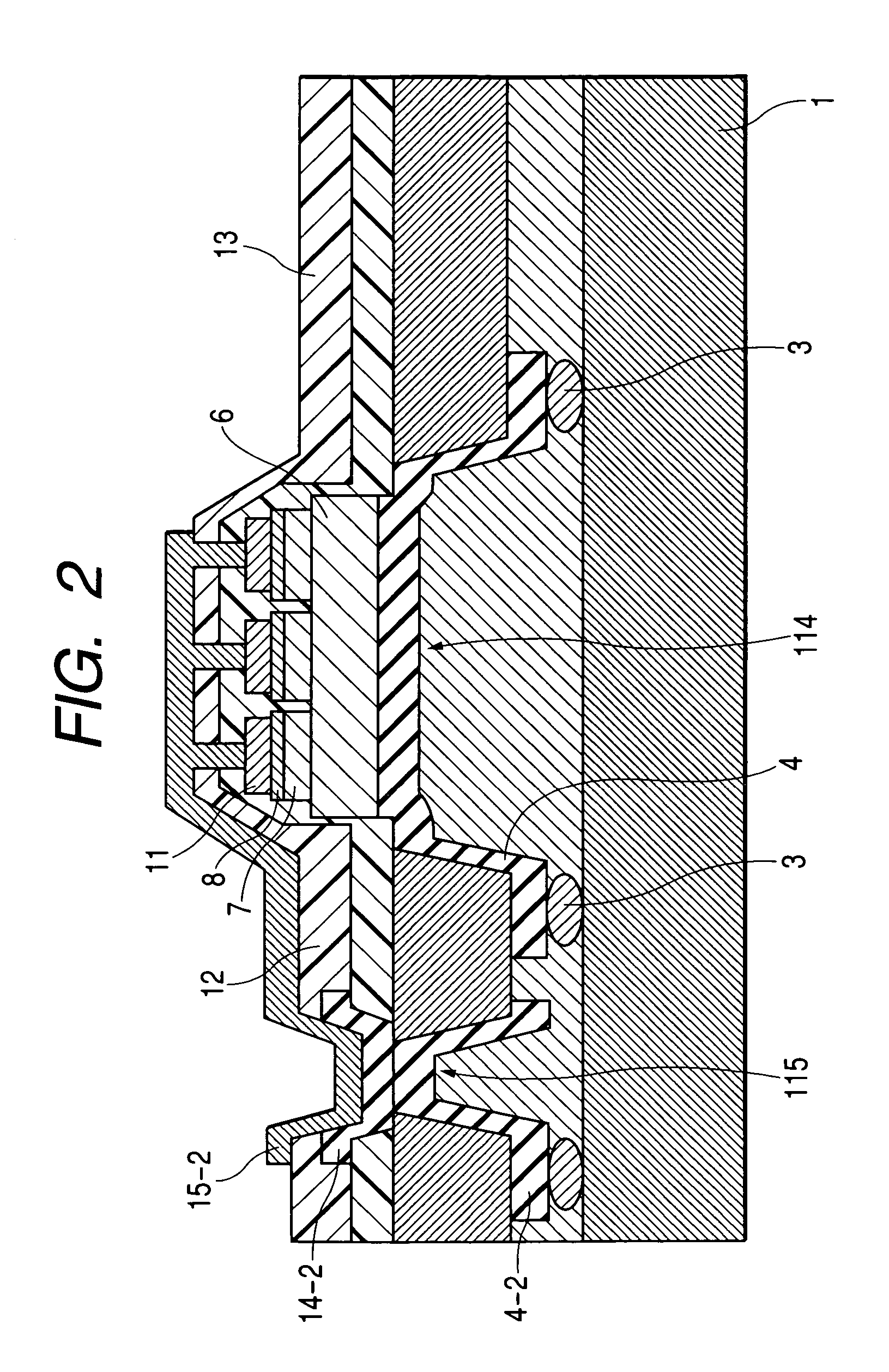
[0046]The basic concept to achieve the objects of the present invention is described below. In a HBT-used MMIC, a first, second and third via holes are formed from the bottom surface of the MMIC. This makes it possible to mount the MMIC face up on a power amplifier module plate. Thus, capacitances parasitic to the connections between the MMIC's conductor layers and the module plate can be reduced. In addition, the variability of the capacitance parasitic to each conductor layer can be limited. This makes it possible to prepare a power amplifier module superior in high frequency characteristic.
[0047]In this case, if the first via hole is located so as to face the HBT, the area used to metal bums on the bottom surface of the MMIC can be minimized. This makes it possible to realize a smaller MMIC and therefore a smaller power amplifier module using the MMIC.
[0048]FIG. 14 shows a typical example of a power amplifier. Like common power amplifiers, HBTs Q1 and Q2 are used as emitter-groun...
PUM
 Abstract
Description
Claims
Application Information