Semiconductor device and manufacturing method thereof

a semiconductor and semiconductor technology, applied in the field of semiconductor devices, can solve the problems of deteriorating connection state between the electrodes of the protruding portion and their corresponding metal wires, inability to satisfactorily transfer ultrasonic sound to the metal wires and electrodes, and cracks in the upper semiconductor chips, so as to prevent the occurrence of cracks and ensure the connection

Inactive Publication Date: 2006-07-04
LAPIS SEMICON CO LTD
View PDF12 Cites 7 Cited by
  • Summary
  • Abstract
  • Description
  • Claims
  • Application Information

AI Technical Summary

Benefits of technology

[0012]With the foregoing in view, it is thus an object of the present invention to provide a semiconductor device capable of, when a plurality of semiconductor chips are laminated with being shifted from one another, improving connections between electrodes of a protruding portion of each semiconductor chip and their corresponding metal wires and suppressing degradation of each semiconductor chip due to stress applied upon resin encapsulation.
[0014]In the semiconductor device according to the present invention, the second semiconductor chip (lamination side) is fixed to the first semiconductor chip (laminated side) and even to the support member. That is, the second semiconductor chip fixes a portion (protruding portion) that protrudes or extends out from the first semiconductor chip, to the support member, whereby a protruding portion of the semiconductor chip is supported by the support member. Since the support member exists in space defined between the protruding portion of the second semiconductor chip and a lead frame (die pad section and lead terminal sections), heat applied from a heat coma is satisfactorily transferred from the lead frame to the protruding portion of the second semiconductor chip through the support member even when electrodes are placed at the protruding portion. Also since the support member exists between the protruding portion of the second semiconductor chip and the lead frame, an ultrasonic sound can be transferred to metal wires satisfactorily. As a result, the electrodes of the protruding portion and the metal wires can be reliably connected.
[0015]Since the support member exists in the space defined between the protruding portion and the lead frame, the flowing of a resin into the space between the protruding portion and the lead frame can be suppressed in a resin encapsulating process. Consequently, it is possible to prevent the occurrence of cracks in the second semiconductor chip by application of excessive stress to the protruding portion in the resin encapsulating process.

Problems solved by technology

When electrodes are laid out at the protruding portion, heat from the lead frame is hard to be transferred to the protruding portion upon wire bonding, and an ultrasonic sound applied to metal wires and electrodes also escapes to the space, so that the ultrasonic sound is not satisfactorily transferred to the metal wires and electrodes.
As a result, there is a possibility that the state of connections between the electrodes of the protruding portion and their corresponding metal wires will be deteriorated.
There is also a fear that upon resin encapsulation, a resin flows into the space defined between the protruding portion and the lead frame, so that the protruding portion undergoes stress, thus producing a crack in the upper semiconductor chip.
The semiconductor device described in the patent document 2 has the fear that although it has the effect of causing the lowermost semiconductor chip to directly contact the heat coma to thereby improve the transfer of heat, stress is applied to protruding portions of the respective semiconductor chips upon resin sealing, thus producing cracks in these semiconductor chips.

Method used


Image

  • Semiconductor device and manufacturing method thereof
  • Semiconductor device and manufacturing method thereof
  • Semiconductor device and manufacturing method thereof

Examples


Embodiment Construction

[0032]Preferred embodiments of the present invention will be described hereinbelow with reference to the accompanying drawings.

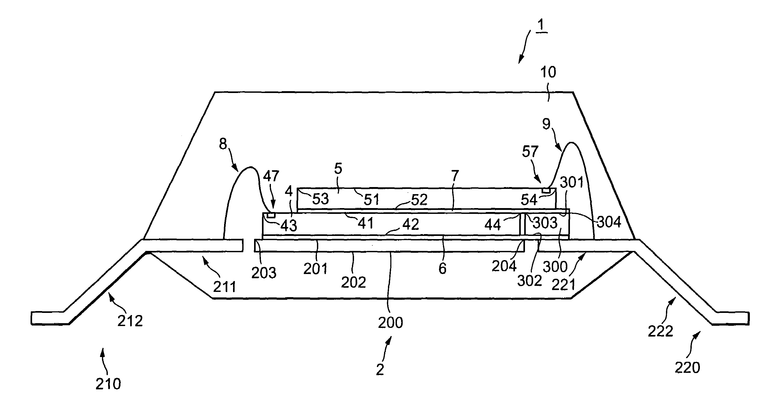
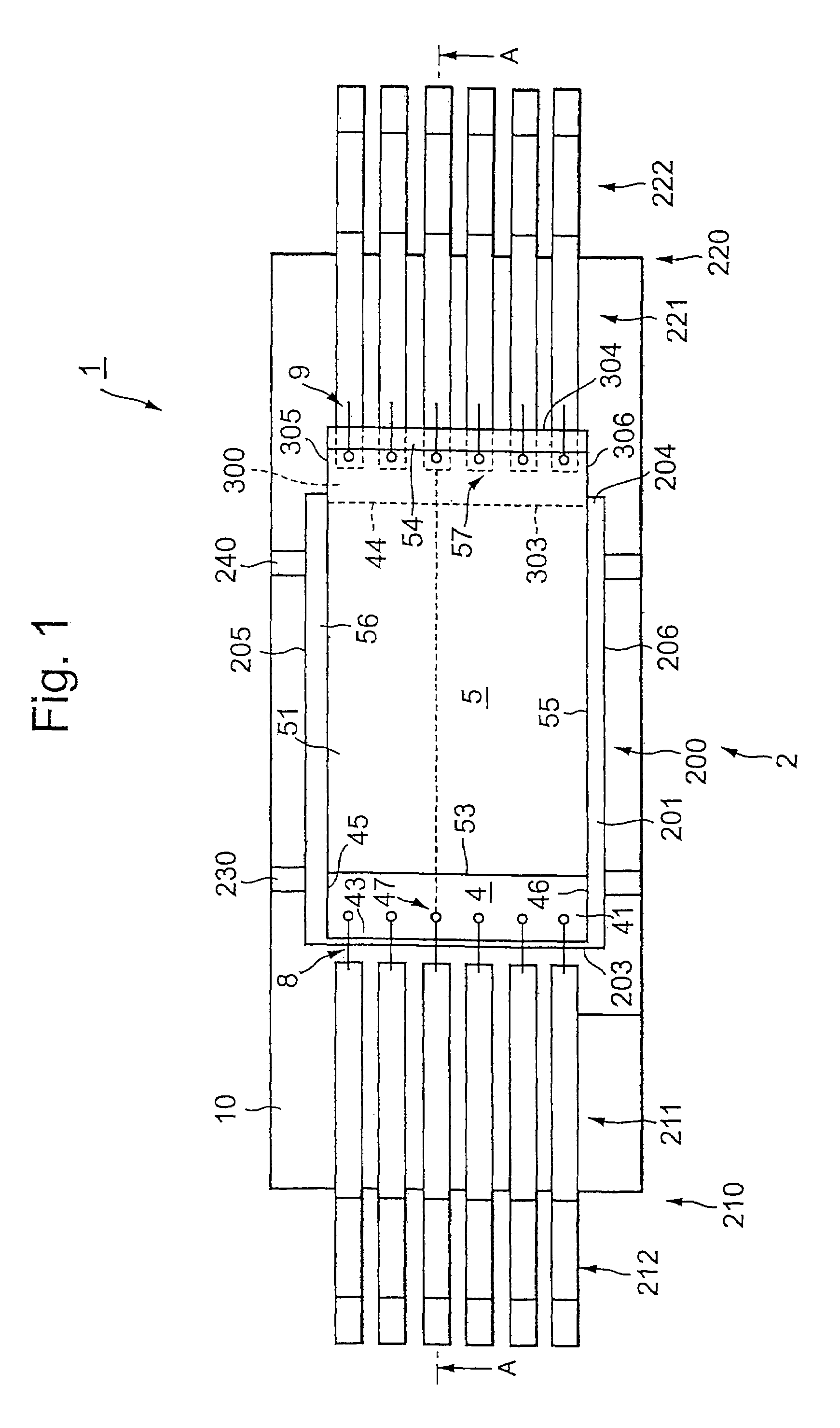
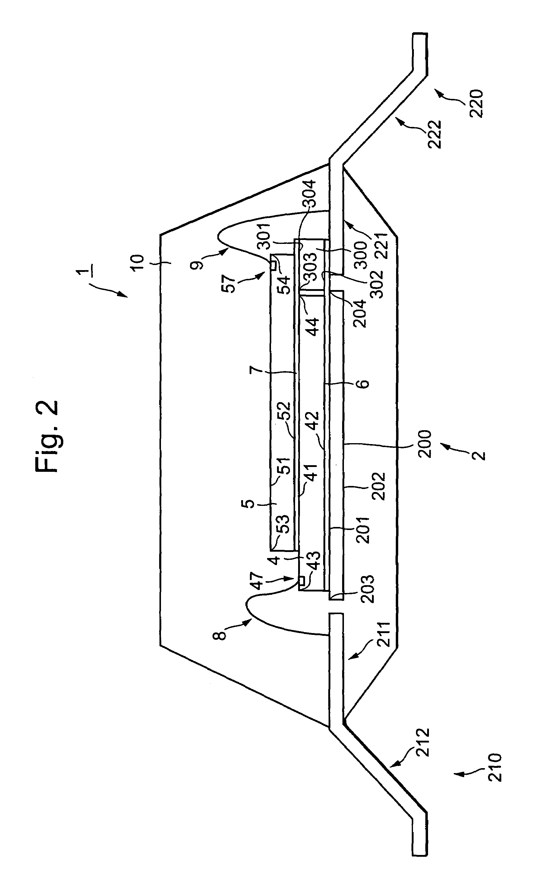
[0033]FIG. 1 is a top perspective diagram (corresponding to a diagram from which an upper resin encapsulating body is omitted) of a semiconductor device 1 according to a first embodiment of the present invention, and FIG. 2 is a cross-sectional view taken along line A—A of FIG. 1, respectively. The semiconductor device 1 is a semiconductor memory device, for example.

[0034]The semiconductor device 1 comprises a lead frame 2 having a die pad section 200 and lead terminal sections 210 and 220, semiconductor chips 4 and 5, a support member 300 and wiring sections 8 and 9 made up of a plurality of metal wires.

[0035]The lead frame 2 includes the die pad section 200, the lead terminal sections 210 and 220 disposed on both sides of the die pad section 200 with a predetermined interval (0.5 mm, for example) defined therebetween, and support portions 230 and 240 for s...


PUM


Abstract

A semiconductor device includes a die pad section, a first semiconductor chip having a surface formed with a first electrode section and a back surface fixed to the die pad section, a second semiconductor chip having a surface formed with a second electrode section and a back surface fixed to the surface of the first semiconductor chip, a support member having a surface fixed to the back surface of the second semiconductor chip and a back surface fixed to the die pad section, lead terminal sections respectively electrically connected to the first and second electrode sections, and a resin encapsulating body that seals the die pad section, the first and second semiconductor chips and the support member.

Description

BACKGROUND OF THE INVENTION[0001]1. Field of the Invention[0002]The present invention relates to a semiconductor device and a manufacturing method thereof, and particularly to a semiconductor device of a semiconductor chip laminated type wherein a plurality of semiconductor chips are laminated.[0003]2. Description of the Related Art[0004]A conventional bonding device and a semiconductor device both aimed at improving bonding processing of metal wires have been described in the following patent documents 1 and 2 respectively. The patent document 1 describes the bonding device in which a lead terminal mounting or placement surface of a heat coma is slanted. Since lead terminals are satisfactorily brought into contact with the mounting surface of the heat coma even if the lead terminals have warpage upon fixing the lead terminals to the mounting surface of the heat coma by a window clamper in the bonding device, heat applied from the heat coma is satisfactorily transferred to the lead ...

Claims


Application Information

Patent Timeline
Patent Type & Authority Patents(United States)
IPC IPC(8): H01L23/495H01L23/48H01L23/52H01L29/40H01L21/607H01L25/18H01L25/065H01L25/07
CPCH01L23/49575H01L24/85H01L2224/32245H01L2224/32145H01L2224/48091H01L2224/48247H01L2224/48465H01L2224/49175H01L2224/73265H01L2224/85186H01L2224/92H01L2224/92247H01L2225/06562H01L2924/01006H01L2924/01014H01L2924/01074H01L2924/01082H01L24/49H01L2924/01033H01L2924/01005H01L2924/00014H01L24/48H01L2224/78H01L2924/00H01L2924/00012H01L2224/451H01L2924/181H01L2224/85205H01L24/45H01L24/73H01L2924/00015H01L2224/05599
Inventor ICHIKAWA, SUNJI
Owner LAPIS SEMICON CO LTD
Why Eureka
Try Eureka