Image display device incorporating driver circuits on active substrate and other methods to reduce interconnects

a driver circuit and active substrate technology, applied in the field of flat panel displays, can solve the problems of increased cost of display manufacture, additional sources of defects, defective pixels, etc., and achieve the effect of reducing the number of wire interconnections of the devi

Inactive Publication Date: 2006-07-04
SONY CORP +1
View PDF91 Cites 69 Cited by
  • Summary
  • Abstract
  • Description
  • Claims
  • Application Information

AI Technical Summary

Benefits of technology

[0008]The invention provides a flat panel display device having driver integrated circuits incorporated on the same substrate having the active region and including other methods to reduce the number of wire interconnects for the device.

Problems solved by technology

As the resolution of the device increases, the number of interconnects (i.e., discrete wires and metal lines) coupling to the active display region increases, the cost of the manufacture of the display increases and additional sources for defects are introduced.
Each connection from the driver ICs to the active display region 20 controls a given column or line such that a connection defect at any point from the driver IC to the active display region 20 may result in a defective pixel.
Furthermore, additional metal lines or leads passing through the vacuum seal increase the likelihood of outgassing or other compromise of the vacuum seal.
Thus, it becomes increasingly difficult to reliably connect the driver ICs to the active display region 20 without compromising the display performance.

Method used


Image

  • Image display device incorporating driver circuits on active substrate and other methods to reduce interconnects
  • Image display device incorporating driver circuits on active substrate and other methods to reduce interconnects
  • Image display device incorporating driver circuits on active substrate and other methods to reduce interconnects

Examples


Embodiment Construction

[0040]The following description is not to be taken in a limiting sense, but is made merely for the purpose of describing the general principles of the preferred embodiments. The scope of the invention should be determined with reference to the claims.

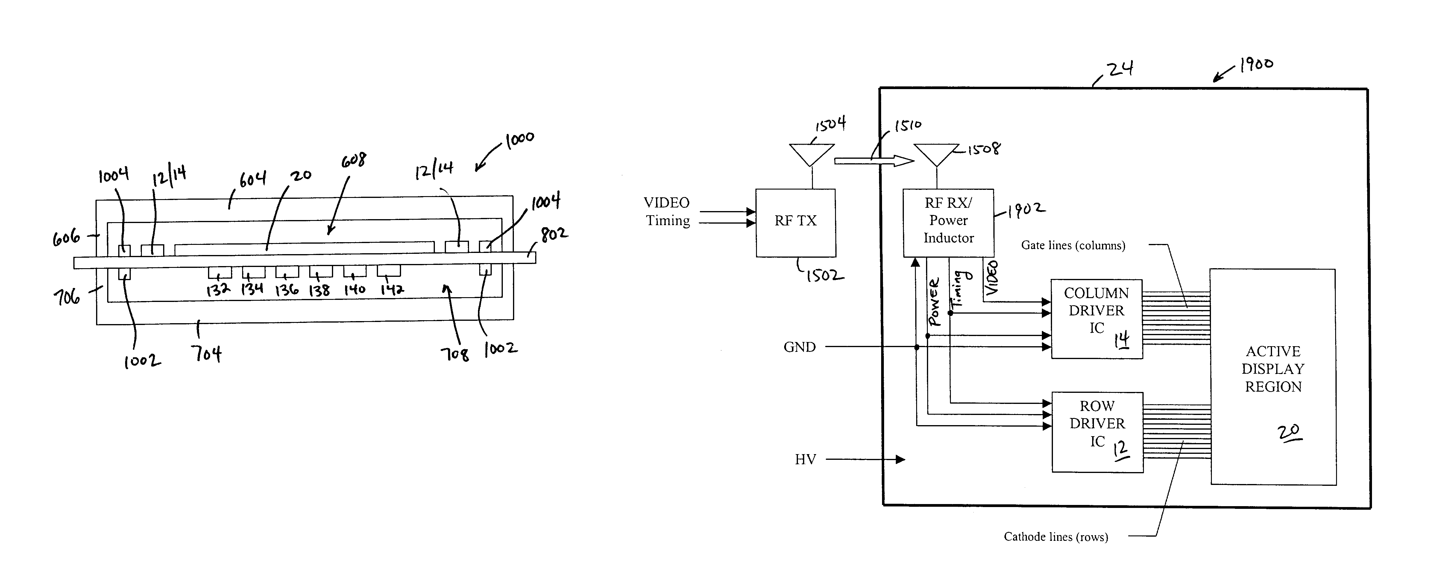
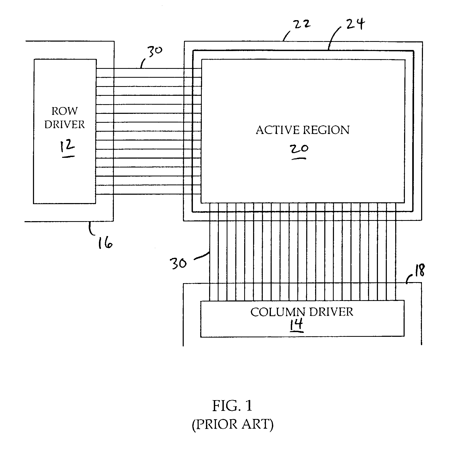
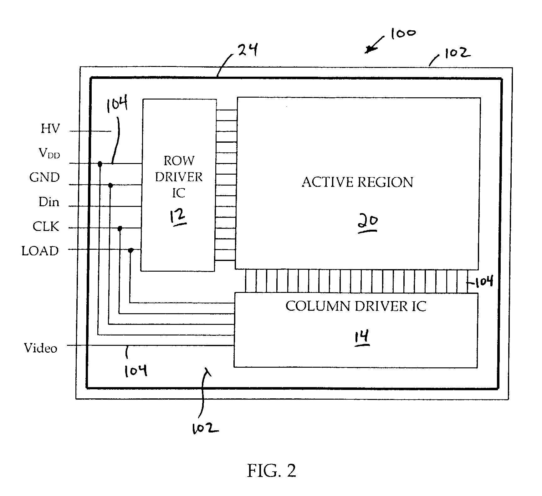
[0041]In accordance with several embodiments of the present invention, a vacuum-sealed flat panel display device, such as a field emission display (FED) or a plasma display, is provided having driver integrated circuits (ICs) incorporated on the same substrate as the active display region of the display within the vacuum-sealed volume in order to reduce the number of interconnects for the device. Thus, advantageously, the number of wire interconnects passing through the vacuum seal, e.g., frit seal, is reduced. Furthermore, as the display resolution increases, the number of interconnects passing through the vacuum seal does not increase.

[0042]Generally, embodiments of the invention in which driver integrated circuitry is incorporated on...


PUM


Abstract

Flat panel displays, such as field emission displays (FEDs), plasma displays, liquid crystal displays (LCDs), and electroluminescent displays (ELs), are provided incorporating driver circuitry on the same substrate as the active display region of the display device and further reducing through-vacuum and substrate-to-substrate interconnects. In one implementation, an image display device comprises a substrate; an active display region formed on the substrate and including addressable rows and columns defining pixels; and one or more driver ICs on the substrate, respective outputs of each driver IC coupled to respective ones of the addressable rows and columns, the driver ICs adapted to drive the active display region to display an image. The device also comprises a wireless receiver coupled to the driver ICs, the wireless receiver adapted to wirelessly receive a wireless signal including an input video signal for display and couple the input video signal to the driver ICs.

Description

[0001]This application is related to U.S. patent application Ser. No. 10 / 404,712, filed concurrently herewith, of Miyazaki, entitled “IMAGE DISPLAY DEVICE INCORPORATING DRIVER CIRCUITS ON ACTIVE SUBSTRATE TO REDUCE INTERCONNECTS”, the entirety of which is incorporated herein by reference.BACKGROUND OF THE INVENTION[0002]1. Field of the Invention[0003]The present invention relates generally to flat panel displays (FPDs), and more specifically to driving flat panel displays. Even more specifically, the present invention relates to driving high-resolution flat panel displays.[0004]2. Discussion of the Related Art[0005]Flat panel displays (FPDs), such as plasma displays and liquid crystal displays (LCDs), are becoming increasingly popular for use in display device technologies, particularly for computer monitor and television type thin displays. Furthermore, field emission displays (FEDs) are being developed for mass consumer applications.[0006]Such flat panel displays operate by addres...

Claims


Application Information

Patent Timeline
Patent Type & Authority Patents(United States)
IPC IPC(8): G09G3/10G09G5/00G09G3/20G09G3/22H01J17/34H01J17/36H01J29/96H01J29/98
CPCG09G3/20G09G3/22H01J29/98H01J29/96G09G2300/0408
Inventor RUSS, BENJAMIN EDWARDBARGER, JACKKAWASAKI, KENICHI
Owner SONY CORP
Why Eureka
Try Eureka