Precise voltage/current reference circuit using current-mode technique in CMOS technology

a current-mode technique and voltage/current reference technology, applied in the direction of electric variable regulation, process and machine control, instruments, etc., can solve the problem of degrading the accuracy of current referen

Active Publication Date: 2006-07-04
INTEGRATED DEVICE TECH INC
View PDF5 Cites 48 Cited by
  • Summary
  • Abstract
  • Description
  • Claims
  • Application Information

AI Technical Summary

Benefits of technology

[0021]A third transistor, having a current mirror configuration with respect to the first transistor, provides a current equal to the reference current (i.e., (VBE1−VBE2) / R1 +VBE1 / R2) to a third resistor having a resistance R3. This third resistor is connected in series with a third bipolar transistor that exhibits a third base-to-emitter voltage VBE3. As a result, the voltage drop across the third resistor and the third bipolar transistor is equal to VBE3+(R3×(VBE1−VBE2) / R1+R3×VBE1 / R2). This voltage drop is used as a reference voltage. By properly selecting the ratio of the resistances R1, R2 and R3, the reference voltage can be made insensitive to variations in temperature and power supply voltage. Moreover, by properly selecting the ratio of the resistances R1, R2 and R3, the voltage and current reference circuit can be controlled to have a single steady-state operating point.

Problems solved by technology

The process variation of the resistor is a major factor that degrades the precision of the current reference.

Method used


Image

  • Precise voltage/current reference circuit using current-mode technique in CMOS technology
  • Precise voltage/current reference circuit using current-mode technique in CMOS technology
  • Precise voltage/current reference circuit using current-mode technique in CMOS technology

Examples


Embodiment Construction

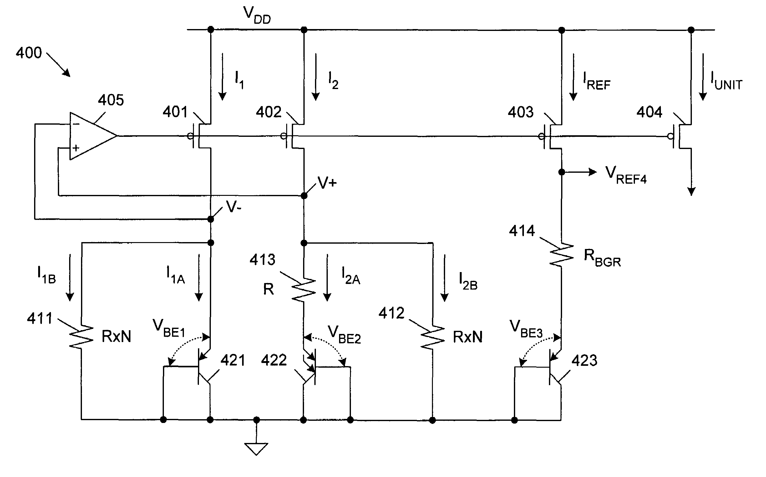
[0029]FIG. 4 is a circuit diagram of an on-chip bandgap voltage and current reference circuit 400 in accordance with one embodiment of the present invention. Voltage / current reference circuit 400 can be used, for example, in CMOS analog / mixed signal chips.

[0030]Voltage reference circuit 400 includes PMOS transistors 401–404, operational amplifier 405, resistors 411–414 and PNP bipolar transistors 421–423. The dimensions of PMOS transistors 401–404 are the same. The sources of PMOS transistors 401–404 are coupled to the VDD voltage supply terminal. The drains of PMOS transistors 401 and 402 are coupled to the “−” and “+” input terminals of operational amplifier 405. The input voltages to the “−” and “+” input terminals of operational amplifier 405 are labeled as input voltages V− and V+, respectively. The output terminal of operational amplifier 405 is coupled to the gates of PMOS transistors 401–404. The currents through PMOS transistors 401, 402, 403 and 404 are designated as I1, I...


PUM


Abstract

A voltage / current reference circuit includes a first bipolar transistor and a second bipolar transistor that exhibit a first voltage drop VBE1 and a second voltage drop VBE2, respectively. A first resistor, having a resistance R1, is configured to draw a first current equal to (VBE1−VBE2) / R1. A second resistor, having a resistance R2, is configured to draw a second current equal to VBE1 / R2. A first transistor supplies the first and second currents to the first and second resistors. A second transistor, having a current mirror configuration with respect to the first transistor, directly provides a reference current equal to (VBE1−VBE2) / R1+VBE1 / R2. A third transistor, having a current mirror configuration with respect to the first transistor, provides a current equal to the reference current to a third resistor having a resistance R3 and a third bipolar transistor that exhibits a third voltage drop VBE3, thereby generating a reference voltage.

Description

FIELD OF THE INVENTION[0001]The present invention relates to a precise voltage / current reference circuit that is insensitive to variations in temperature and power supply voltage. More specifically, the present invention relates to a voltage / current reference circuit using a current-mode technique in CMOS technology.RELATED ART[0002]FIG. 1 is a circuit diagram of a conventional on-chip bandgap voltage reference circuit 100 used in CMOS analog / mixed signal chips. Voltage reference circuit 100 includes PMOS transistors 101–102, operational amplifier 105, resistors 111–113 and PNP bipolar transistors 121–122, which are connected as illustrated. Resistors 111, 112 and 113 have resistances of R1, R2 and R3, respectively. The input voltages to the “+” and “−” input terminals of operational amplifier 105 are labeled as input voltages V+ and V−, respectively. The base-to-emitter voltage of bipolar transistor 121 is designated VBE1, and the base-to-emitter voltage of bipolar transistor 122 i...

Claims


Application Information

Patent Timeline
Patent Type & Authority Patents(United States)
IPC IPC(8): G05F1/10G05F3/30
CPCG05F3/30
Inventor OU-YANG, QINGYANG, HOWARDGU, YUFEI
Owner INTEGRATED DEVICE TECH INC
Why Eureka
Try Eureka