Apparatus and method for making a low capacitance artificial nanopore

a nanopore, low capacitance technology, applied in the field of nanopores, can solve the problems of difficult and problematic use of external packaging alone to produce a small liquid contact area, and low resistivity of silicon

Inactive Publication Date: 2006-07-11
AGILENT TECH INC
View PDF5 Cites 101 Cited by
  • Summary
  • Abstract
  • Description
  • Claims
  • Application Information

AI Technical Summary

Problems solved by technology

A problem with artificial nanopores fabricated on a silicon frame is that silicon is a semiconductor and has low resistivity, typically in the range of 1–50 Ohm-cm, which is much lower than the resistivity of a true insulator such as silicon nitride or silicon dioxide.
But using external packaging alone to produce a small liquid contact area is often difficult and problematic, and that approach ignores the need to place low-capacitance electrical leads on the surface of the insulator layer over the silicon frame.
However, cited references or art are not admitted to be prior art to this application.

Method used


Image

  • Apparatus and method for making a low capacitance artificial nanopore
  • Apparatus and method for making a low capacitance artificial nanopore
  • Apparatus and method for making a low capacitance artificial nanopore

Examples


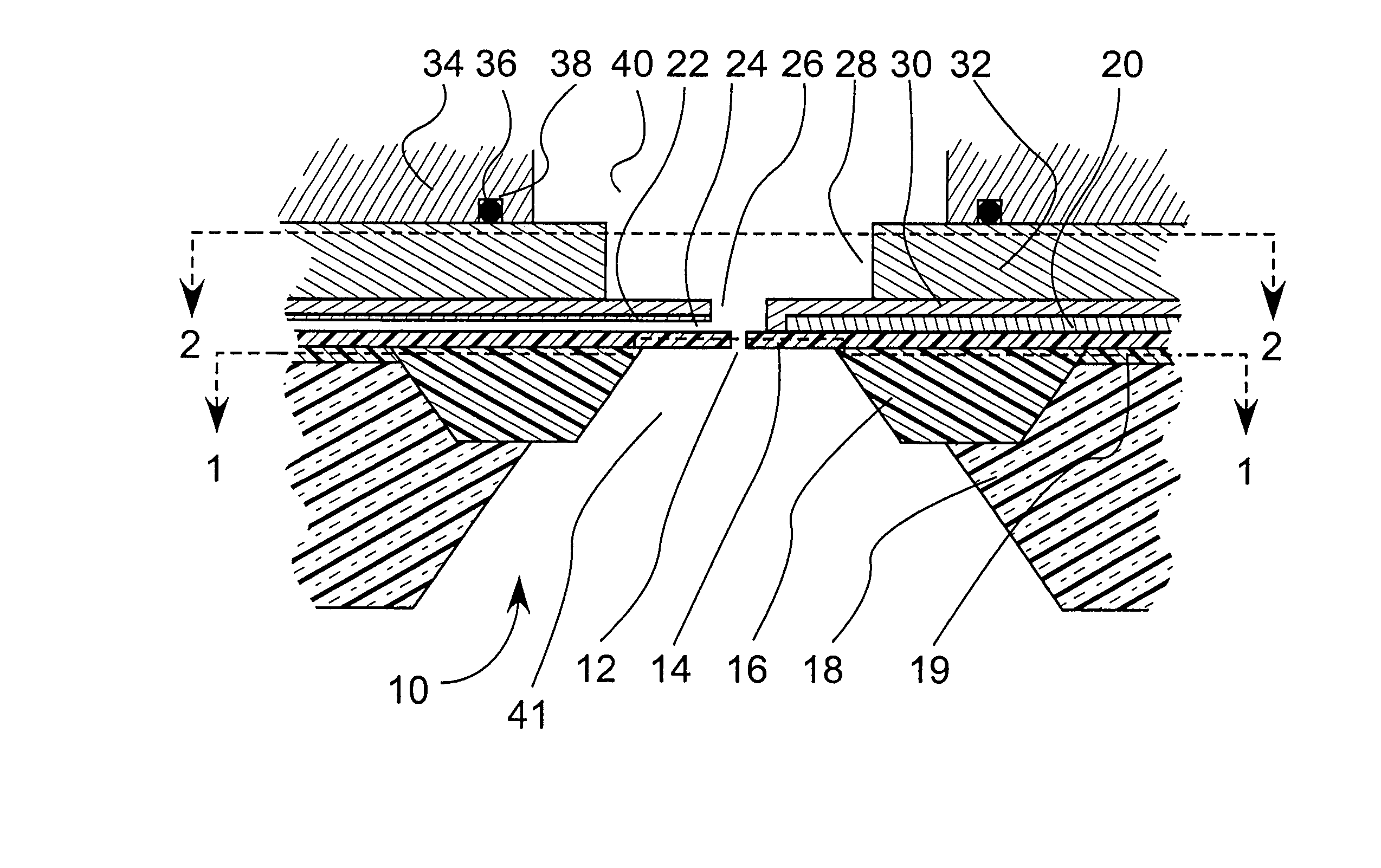
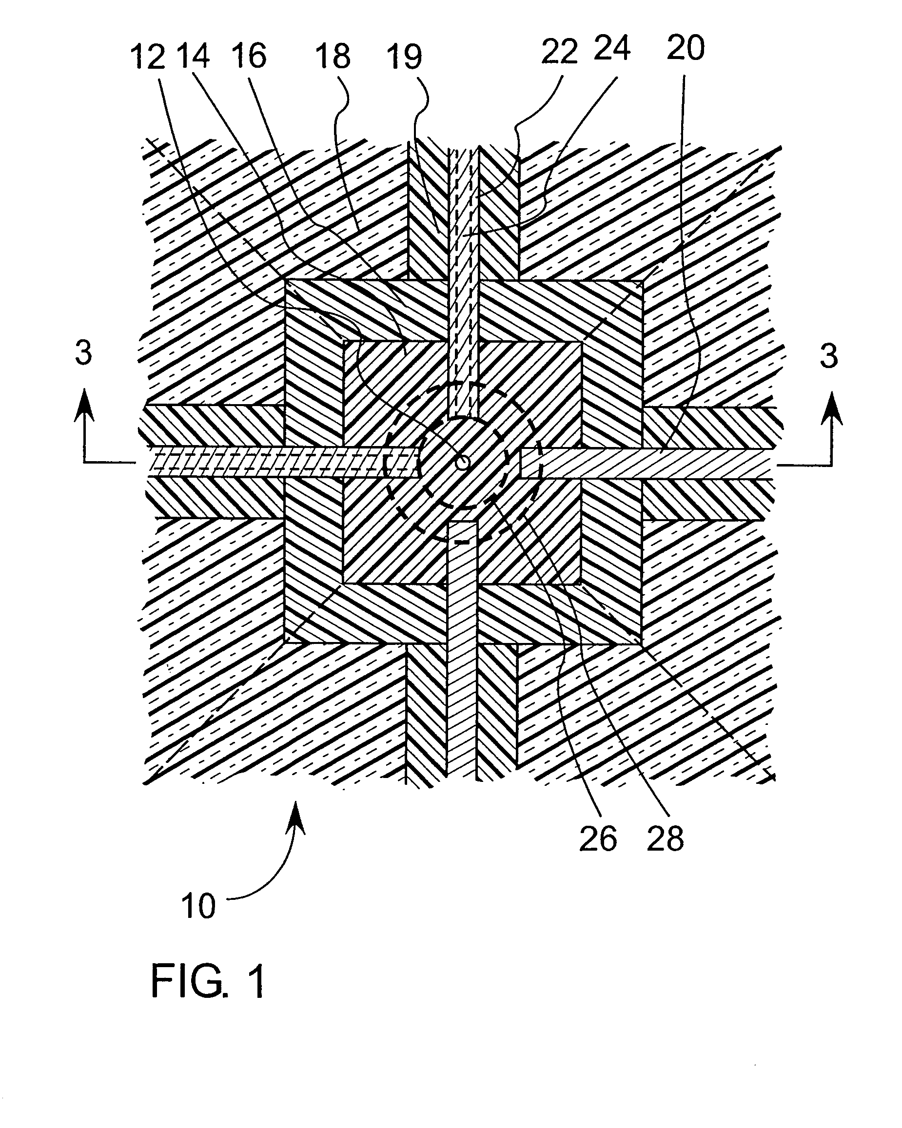
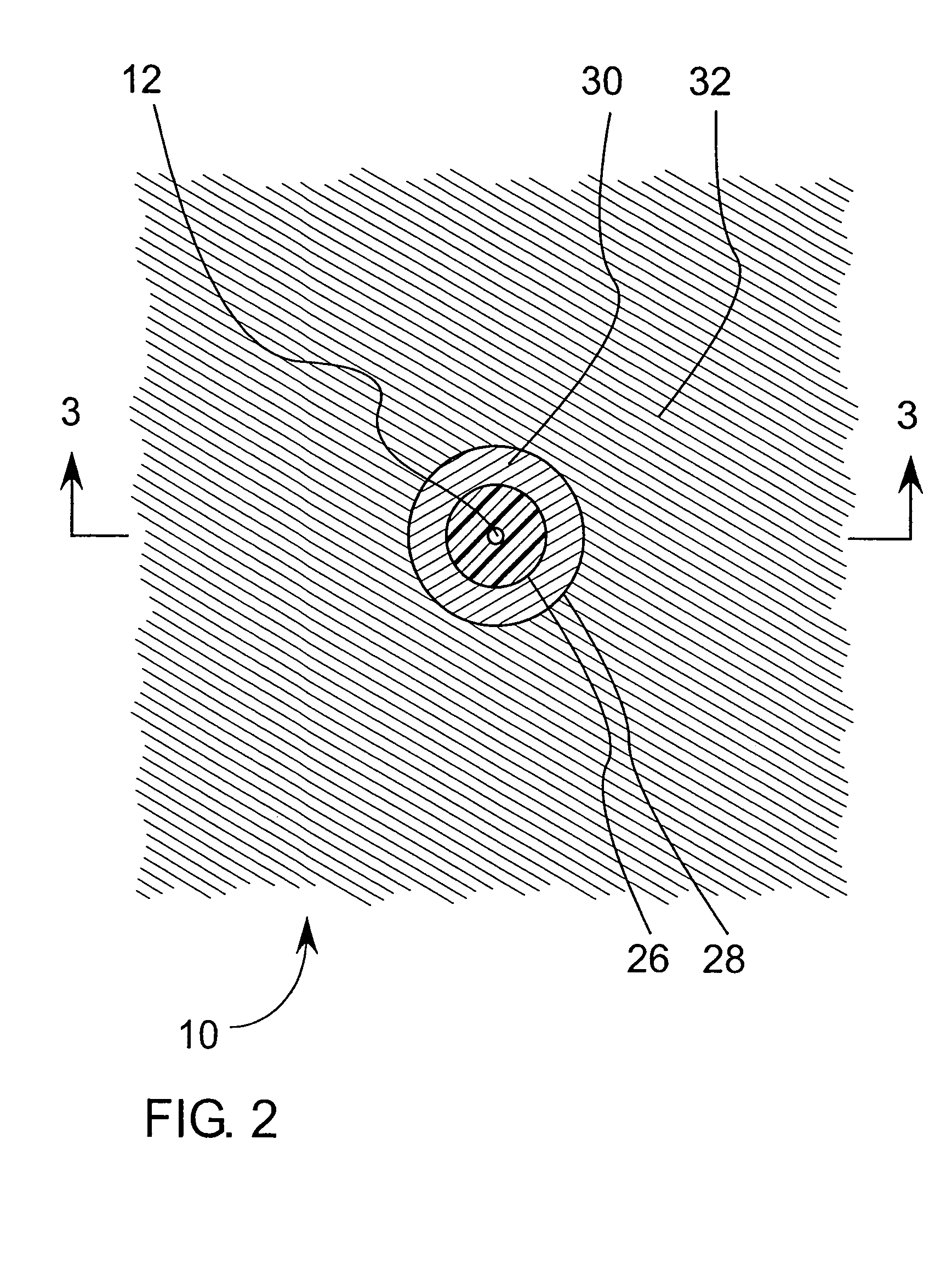
Embodiment Construction

[0039]Before describing the present invention in detail, it is to be understood that this invention is not limited to specific compositions, method steps, or equipment, as such may vary. It is also to be understood that the terminology used herein is for the purpose of describing particular embodiments only, and is not intended to be limiting. Methods recited herein may be carried out in any order of the recited events that is logically possible, as well as the recited order of events.

[0040]Unless defined otherwise below, all technical and scientific terms used herein have the same meaning as commonly understood by one of ordinary skill in the art to which this invention belongs. Still, certain elements are defined herein for the sake of clarity. In the event that terms in this application are in conflict with the usage of ordinary skill in the art, the usage herein shall be controlling.

[0041]Where a range of values is provided, it is understood that each intervening value, to the t...


PUM

PropertyMeasurementUnit
thicknessaaaaaaaaaa
thickaaaaaaaaaa
thicknessaaaaaaaaaa

Abstract

An apparatus and method for making a nanopore chip exhibiting low capacitance. The apparatus provides a thin diaphragm on a rigid semiconductor frame suitable for nanopore fabrication, the diaphragm having associated thicker insulator regions to reduce capacitance. Also disclosed is a method of making the apparatus.

Description

TECHNICAL FIELD[0001]The invention relates generally to the field of nanopores and more particularly to an apparatus and method for making a low capacitance artificial nanopore.BACKGROUND[0002]Manipulating matter at the nanometer scale is important for many electronic, chemical and biological advances (See Li et al., “Ion beam sculpting at nanometer length scales”, Nature, 412: 166–169, 2001). Such techniques as “ion beam sculpting have shown promise in fabricating molecule scale holes and nanopores in thin insulating membranes. These pores have also been effective in localizing molecular-scale electrical junctions and switches (See Li et al., “Ion beam sculpting at nanometer length scales”, Nature, 412: 166–169, 2001).[0003]Artificial nanopores have been fabricated by a variety of research groups with a number of materials. Generally, the approach is to fabricate these nanopores in a solid-state material or a thin freestanding diaphragm of material supported on a frame of thick sil...

Claims


Application Information

Patent Timeline
Patent Type & Authority Patents(United States)
IPC IPC(8): H01L27/14H01L29/84B82B3/00B81B1/00B81C1/00B82B1/00
CPCG01N33/48721B81C1/00087B81B2201/058B81B2203/0127B81B2203/0338
Inventor BARTH, PHILLIP W.
Owner AGILENT TECH INC
Why Eureka
Try Eureka