Optical waveguide and fabricating method thereof
a technology of optical waveguides and fabrication methods, applied in the field of optical waveguides, can solve the problems of large propagation loss, complicated node configuration, and low efficiency, and achieve the effects of reducing polarization dependency, reducing distortion stress against heat, and reducing polarization dependency
- Summary
- Abstract
- Description
- Claims
- Application Information
AI Technical Summary
Benefits of technology
Problems solved by technology
Method used
Image
Examples
first modification
(First Modification)
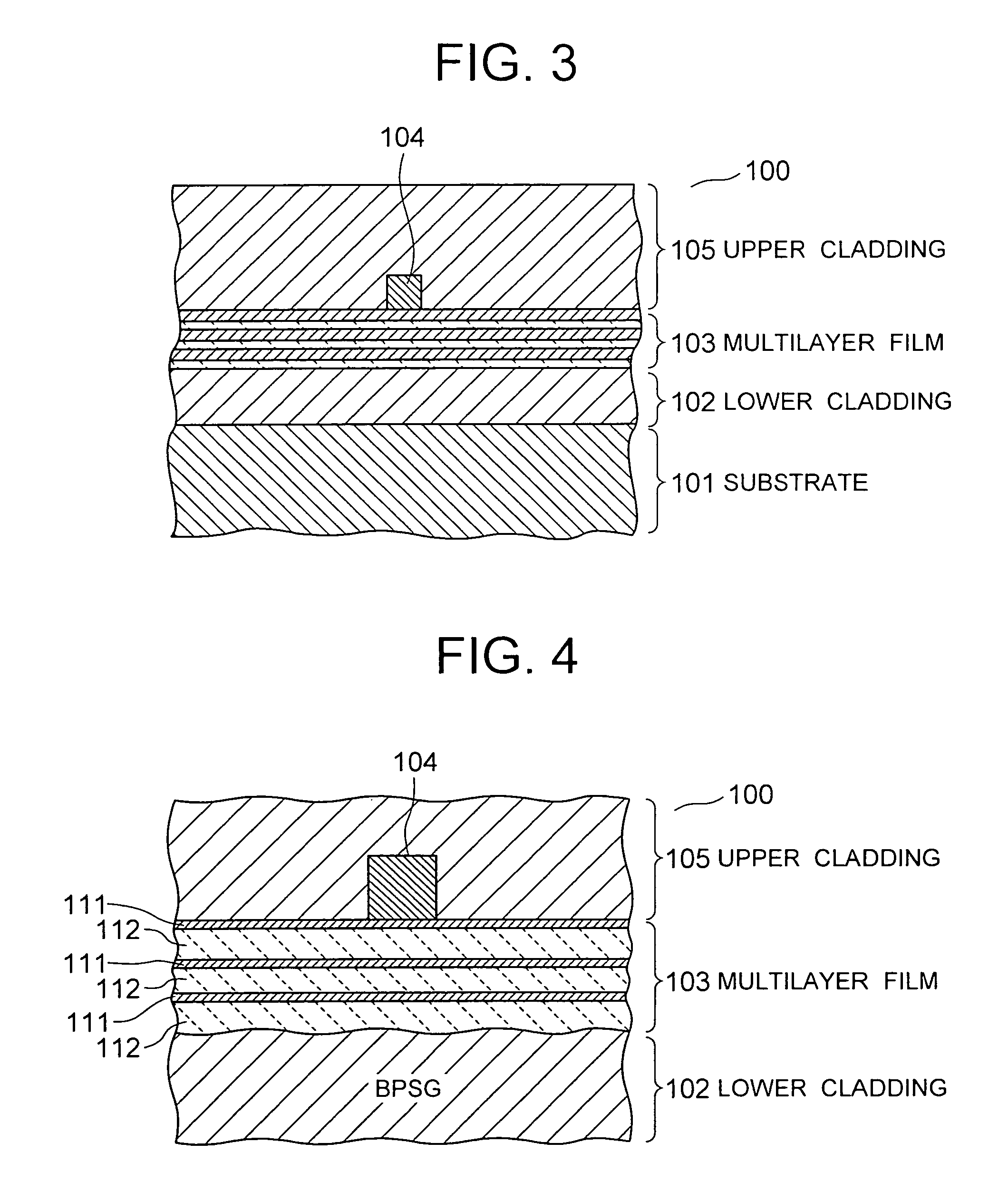
[0048]FIG. 6 shows the main part of an optical waveguide of a first modification according to the present invention. The multilayer films 103 in the embodiments shown in FIG. 3 and in FIG. 6 are different in their multilayer configurations formed by combining multiple materials having different film thickness. In the embodiment shown in FIG. 3, the film thickness of the multiple films 111 are set to be equal, and the film thickness of the other multiple films 112 are set to be equal and thicker than that of the films 111.
[0049]On the other hand, in the embodiment shown in FIG. 6, the multiple films 111 have different film thickness in the vertical direction. The other multiple films 112 have different film thickness in the vertical direction, and are set to be thicker than the film thickness of the films 111. More specifically, an optical waveguide 100B of the first modification is so configured that on the lower cladding 102, a second film 112B1 is formed, and f...
second modification
(Second Modification)
[0050]FIG. 7 shows the main part of an optical waveform of a second modification according to the present invention. An optical waveguide 100C of the second modification is so configured that on the lower cladding 102, a first film 111C1 is formed, and further a second film 112C1 is formed thereon. Then, on the pair of these two kinds of films, another pair of first film 111C2 and second film 112C2 are formed, and further, yet another pair of first film 111C3 and second film 112C3 are formed thereon. In this way, the order of film arrangement is opposite to the films described above. The lower cladding 102 located right under the first film 111C1 is easily melted by heat, similar to the second film 112. Thereby, a tensile stress in a face direction of the first film 111C1 contributes to the flattening of the surface at the time of cooling after high temperature annealing.
[0051]As described above, the arrangement order of the fist film 111 and the second film 112...
PUM
 Abstract
Description
Claims
Application Information


