Identification and implementation of clock gating in the design of integrated circuits

a technology of integrated circuits and clock gates, applied in computer aided design, program control, instruments, etc., can solve the problems of limited ability to identify and define such registers in digital ics, limit the number of registers that can be gated, and high power consumption, so as to achieve the effect of improving efficiency

Active Publication Date: 2006-07-11
SYNOPSYS INC
View PDF17 Cites 44 Cited by
  • Summary
  • Abstract
  • Description
  • Claims
  • Application Information

AI Technical Summary

Benefits of technology

[0009]Accordingly, according to various embodiments of the invention, there is provided for the identification and implementation of clock gating in an integrated circuit (IC), an inventive method, a computer executable code for implementation of the method, a computer system adapted to implement a clock gating recognition method, and also a visualization tool adapted to implement a method, for highlighting gated clock domains and gated / gate-able registers, intended for use in the design of an integrated circuit. Various embodiments of the invention provide efficiency improvements.

Problems solved by technology

In recent years, the size of integrated circuits (ICs) has dramatically increased in both size and number of transistors, resulting in higher power consumption.
However, the ability to identify and define such registers in digital ICs is limited.
This limits the number of registers that can be gated and thus the amount of power saving.

Method used


Image

  • Identification and implementation of clock gating in the design of integrated circuits
  • Identification and implementation of clock gating in the design of integrated circuits
  • Identification and implementation of clock gating in the design of integrated circuits

Examples


Embodiment Construction

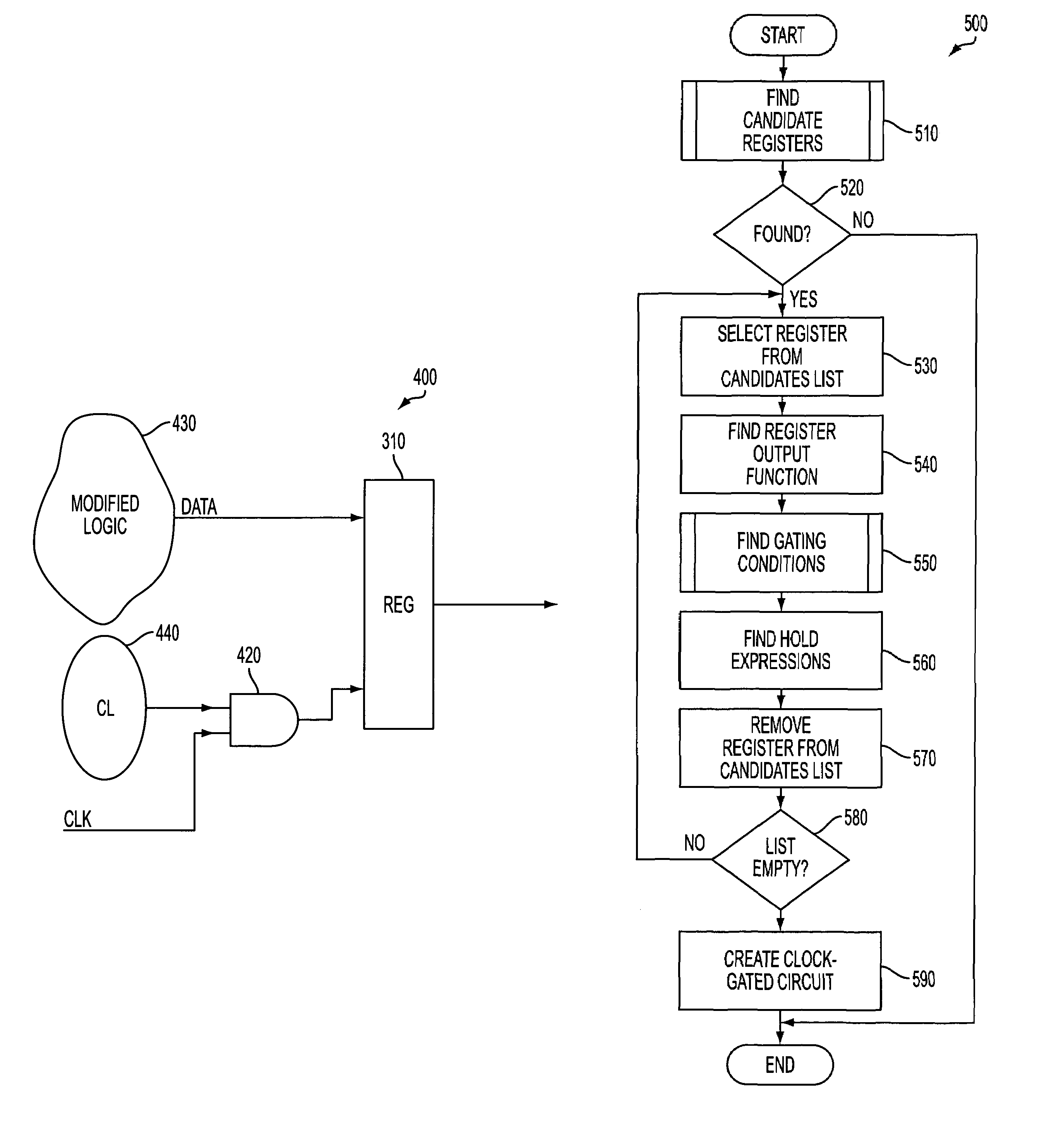
[0023]The invention will now be taught using various exemplary embodiments. Although the embodiments are described in detail, it will be appreciated that the invention is not limited to just these embodiments, but has a scope that is significantly broader. The appended claims should be consulted to determine the true scope of the invention.

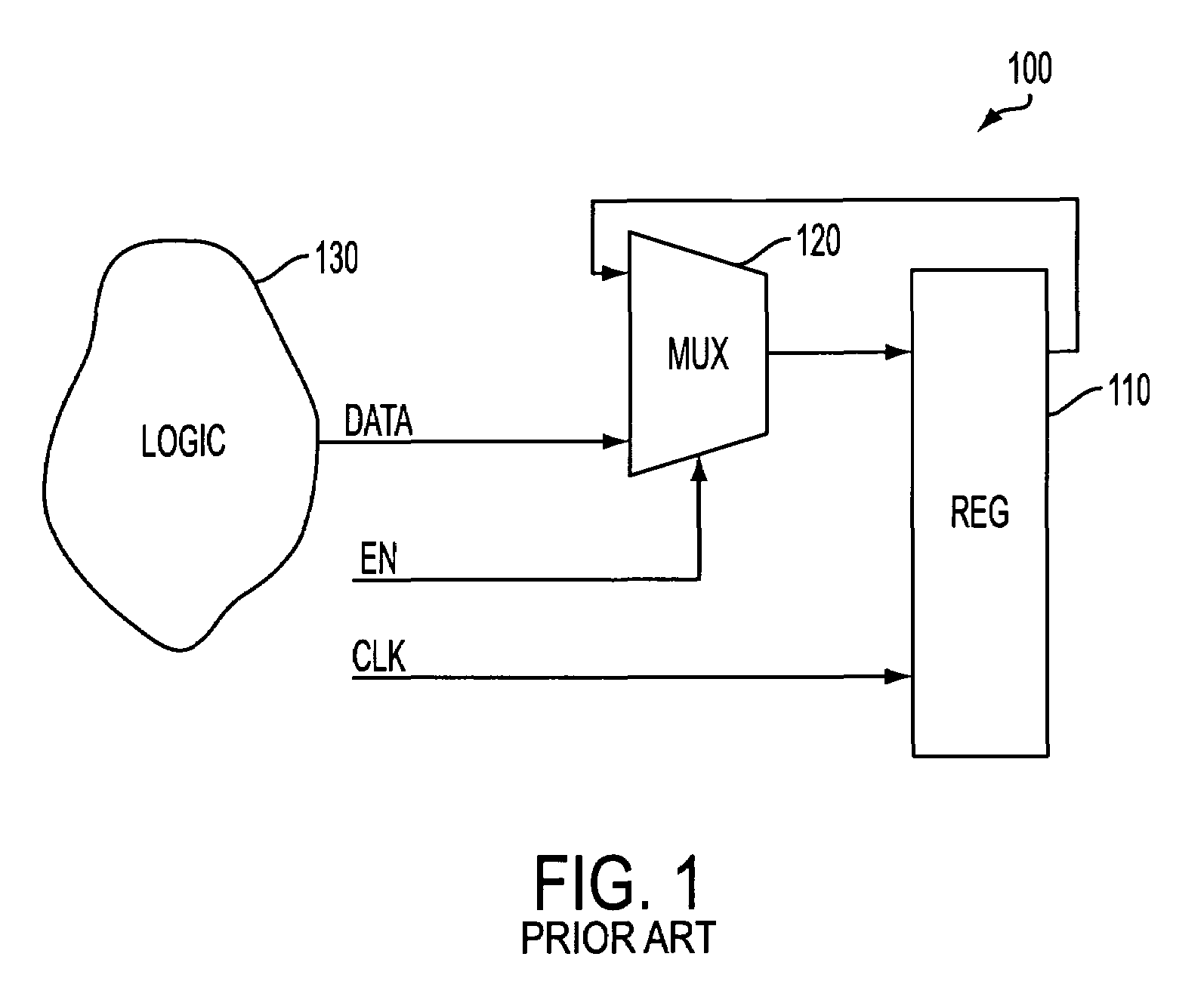
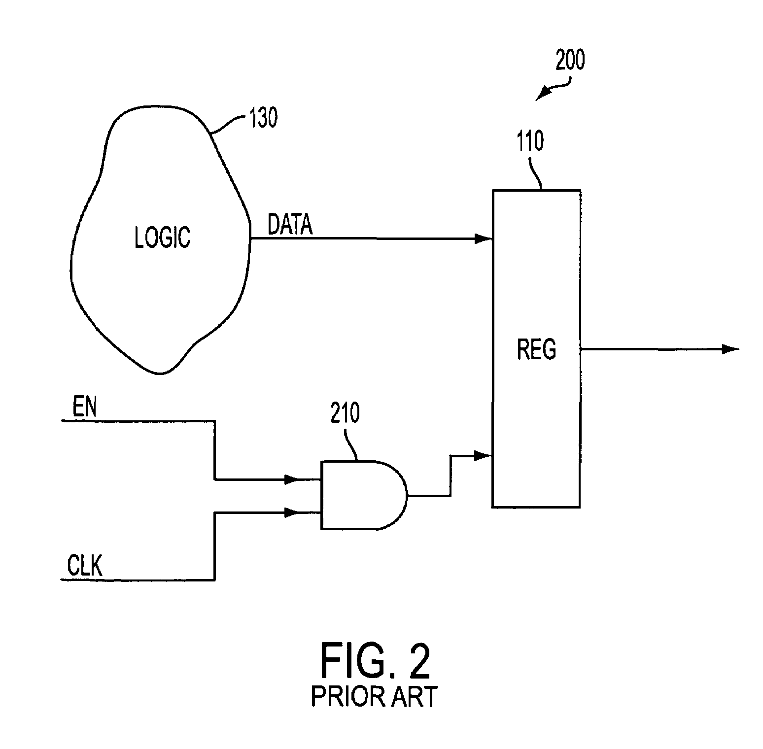
[0024]Reference is now made to FIG. 3 where an exemplary logic circuit 300, prior to the implementation of a clock gating modification in accordance with the disclosed invention, is shown. Circuit 300 is a synchronous load-enabled circuit having a register controlled by a clock “CLK”. The enable signals are generated by combinational logic (CL) 320 which are connected to register 310. The output pins of register 310 are connected to one or more of the input pins of CL 320 through a feedback loop 330. CL 320 comprises combinatorial interconnects of logical gates such as AND gates, OR gates, NAND gates, NOR gates, NOT gates, XOR gates, and Multiplex...


PUM


Abstract

Identification and implementation of clock gating in the design of an integrated circuit (IC) is performed with automated assistance. Electrical power consumption is reduced by clock gating. The automated assistance identifies registers that are candidates for clock gating, and highlights, in the IC design, registers associated with a gated clock domain and the logic blocks driven by these registers.

Description

FIELD OF THE INVENTION[0001]The present invention relates generally to the design of ICs using a gated clock design technique, and more particularly to the low power IC design.BACKGROUND OF THE INVENTION[0002]In recent years, the size of integrated circuits (ICs) has dramatically increased in both size and number of transistors, resulting in higher power consumption. In typical IC designs, the clock distribution network, i.e., the clock tree, can consume from twenty to fifty percent of an IC's total active power. One important technique for reducing power consumption in IC designs is to reduce the power of an IC's clock distribution tree by gating portions of the IC that do not need to be clocked under certain conditions.[0003]This process, known as “clock gating”, disables the clocks fed to logic blocks of the IC when the logic blocks are not currently enabled or otherwise in active use. Power consumption due to the clocking of logic blocks that are not directly involved with the c...

Claims


Application Information

Patent Timeline
Patent Type & Authority Patents(United States)
IPC IPC(8): G06F17/50G06F9/45
CPCG06F17/505G06F2217/62G06F30/327G06F30/396G06F2117/04
Inventor KAPOOR, BHANUCHURIWALA, SANJAYBANERJEE, JOY
Owner SYNOPSYS INC
Why Eureka
Try Eureka