Universal interconnect die

a technology of interconnection die and integrated circuit, which is applied in the direction of semiconductor devices, semiconductor/solid-state device details, electrical apparatus, etc., can solve the problems of difficult interconnection with an external package, semiconductor devices with fixed input/output (i/o) lines, and difficult universal interconnection schemes, so as to achieve flexibility in wiring and prevent long or short leads

Active Publication Date: 2006-07-18
ATMEL CORP
View PDF10 Cites 9 Cited by
  • Summary
  • Abstract
  • Description
  • Claims
  • Application Information

AI Technical Summary

Benefits of technology

[0007]The present invention is a device for electrically interconnecting one or more semiconductor devices to provide for flexibility in wiring and preventing long or shorted leads. The present invention is also a method for fabricating the device and using the same.
[0008]The device has a substrate with a plurality of substantially concentric electrically-conductive paths, each of the plurality of electrically-conductive paths being electrically isolated from each other and formed on a first surface of the substrate. At least one of the plurality of electrically-conductive paths is arranged concentrically so as to substantially span a width of the first surface of the substrate. A plurality of bonding pads is electrically coupled to each of the electrically-conductive paths. The plurality of bonding pads is coupled to one of the electrically-conductive paths and is electrically isolated from bonding pads located on any other electrically-conductive path. Jumper wires may then be used to interconnect various bonding pads, and hence, different electrically-conductive paths. This “jumpering” allows signals to be carried to a distal part of the device without relying on long wire leads and eliminating or greatly minimizing a possibility of electrical shorts. Jumpering also allows for flexibility in wiring arrangements and permits other devices (e.g., active or passive discrete electrical components) to be added to the integrated circuit, thereby providing additional flexibility in electrical design. The entire interconnect device may then be mounted in a standard leadframe product.

Problems solved by technology

As devices become more complex and need to be integrated with additional devices and other apparatus, a universal interconnection scheme becomes more difficult.
Typically, a semiconductor device has fixed input / output (I / O) lines and interconnection with an external package can be difficult.
This difficulty may lead to a redesign of an entire integrated circuit to avoid long lead wires from the device to the package.
Additionally, any lead lines that cross over each other have a potential for developing an electrical short.
Therefore, the interconnection of semiconductor devices with device packages is a major challenge in the art.
Yet, the conductor capacity in the chip greatly lags behind the densification of the silicon devices.

Method used


Image

  • Universal interconnect die
  • Universal interconnect die
  • Universal interconnect die

Examples


Embodiment Construction

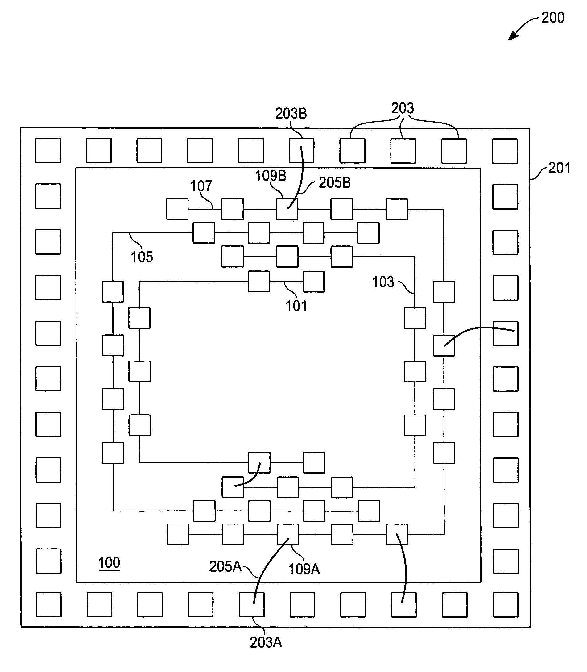
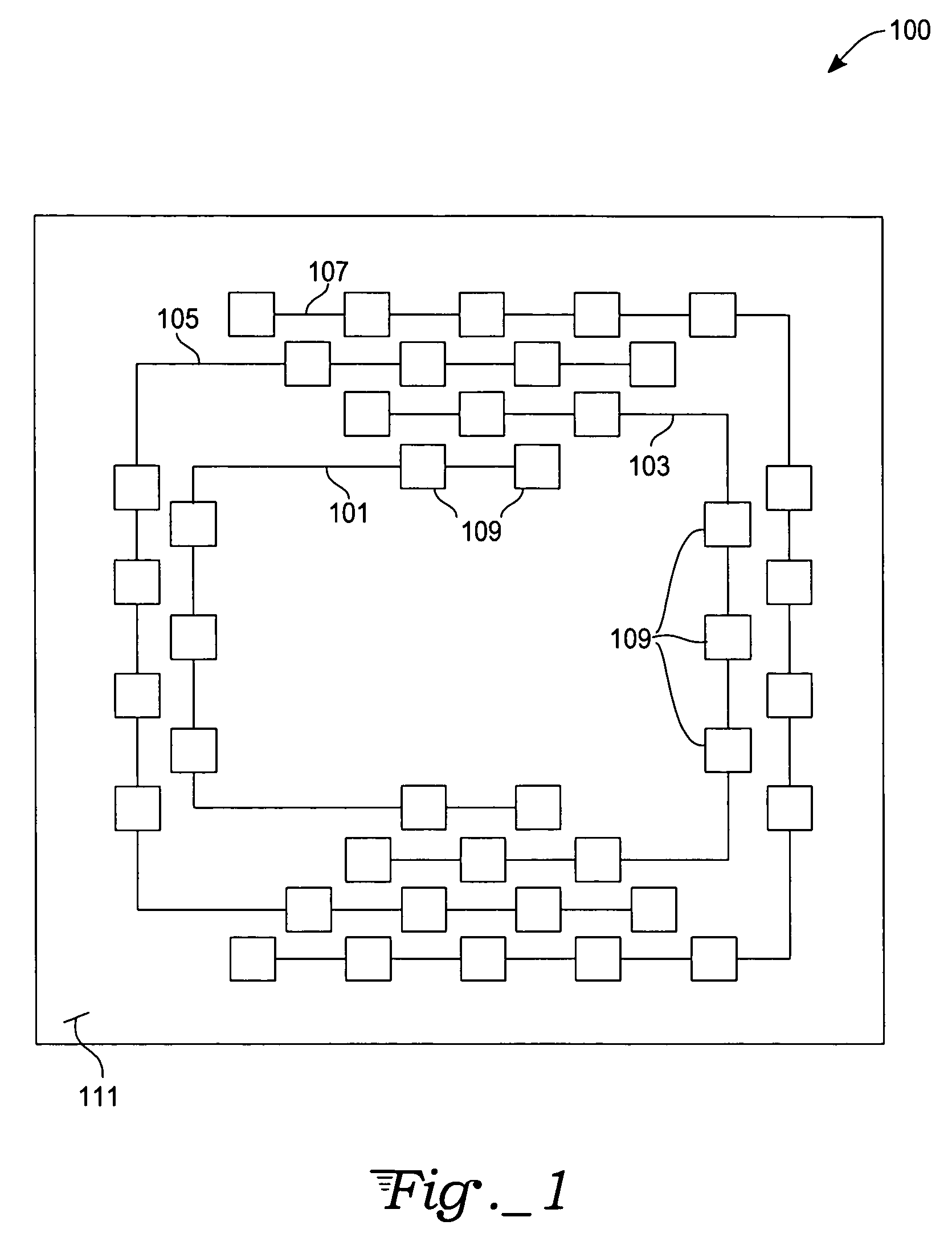
[0022]The present invention will now be described with reference to preferred embodiments thereof. With reference to FIG. 1, a bonding pad interconnection scheme includes a plurality of substantially concentric electrically-conductive coupling paths 101, 103, 105, 107 thus providing various electrical connection paths. Each electrically-conductive coupling path is arranged in a “tier” or series of paths increasing in size with the first tier being the innermost path. Each electrically-conductive coupling path further has a plurality of bonding sites. For example, a first electrically-conductive coupling path 101, in this exemplary embodiment, has seven first-tier bonding pads 109; a second electrically-conductive coupling path 103 has nine second-tier bonding pads, and so on. As a skilled artisan will quickly recognize, a greatly increased number of electrically-conductive bonding pads may be realized by either increasing a number of electrical connection paths and / or closer spacing...


PUM


Abstract

A device for electrically interconnecting one or more semiconductor devices to provide for flexibility in wiring and preventing long or shorted leads and methods for fabricating and using same. The device has a substrate with a plurality of substantially concentric electrically-conductive paths, each of the plurality of electrically-conductive paths being electrically isolated from each other and formed on a first surface of the substrate. At least one of the plurality of electrically-conductive paths is arranged concentrically so as to substantially span a width of the first surface of the substrate. A plurality of bonding pads is electrically coupled to each of the electrically-conductive paths. The plurality of bonding pads is coupled to one of the electrically-conductive paths and is electrically isolated from bonding pads located on any other electrically-conductive path. The entire interconnect device may be mounted in a standard leadframe product.

Description

TECHNICAL FIELD[0001]The present invention relates to an interconnect die for a semiconductor integrated circuit. More particularly, the present invention relates to a universal interconnect die that allows for flexibility in wiring integrated circuits.BACKGROUND ART[0002]Design and manufacturing of semiconductor devices requires cooperative application of a number of diverse technologies. On a macro-scale, a number of these technologies are aimed at first creating the semiconductor devices. Another group of technical disciplines is aimed at packaging the devices. As devices become more complex and need to be integrated with additional devices and other apparatus, a universal interconnection scheme becomes more difficult.[0003]Typically, a semiconductor device has fixed input / output (I / O) lines and interconnection with an external package can be difficult. This difficulty may lead to a redesign of an entire integrated circuit to avoid long lead wires from the device to the package. ...

Claims


Application Information

Patent Timeline
Patent Type & Authority Patents(United States)
IPC IPC(8): H01L23/02H01L23/14H01L23/48H01L23/495H01L23/498H01L25/065
CPCH01L23/49531H01L23/49833H01L23/49838H01L24/06H01L24/49H01L25/0657H01L2924/01079H01L2924/01082H01L2924/10253H01L2924/01023H01L24/48H01L2924/01078H01L2924/01033H01L2924/01029H01L2924/01015H01L2924/12044H01L2924/14H01L23/147H01L2224/05553H01L2224/05624H01L2224/05647H01L2224/48091H01L2224/48145H01L2224/49112H01L2224/49113H01L2225/06506H01L2225/0651H01L2225/06527H01L2924/01005H01L2924/01013H01L2924/01014H01L2924/00014H01L2924/00H01L2224/05554H01L2224/023H01L2224/45099H01L2924/00012H01L2924/0001
Inventor LAM, KEN M.KOVATS, JULIUS A.
Owner ATMEL CORP
Why Eureka
Try Eureka