Methods and apparatus for implementing a power down in a memory device
- Summary
- Abstract
- Description
- Claims
- Application Information
AI Technical Summary
Benefits of technology
Problems solved by technology
Method used
Image
Examples
Embodiment Construction
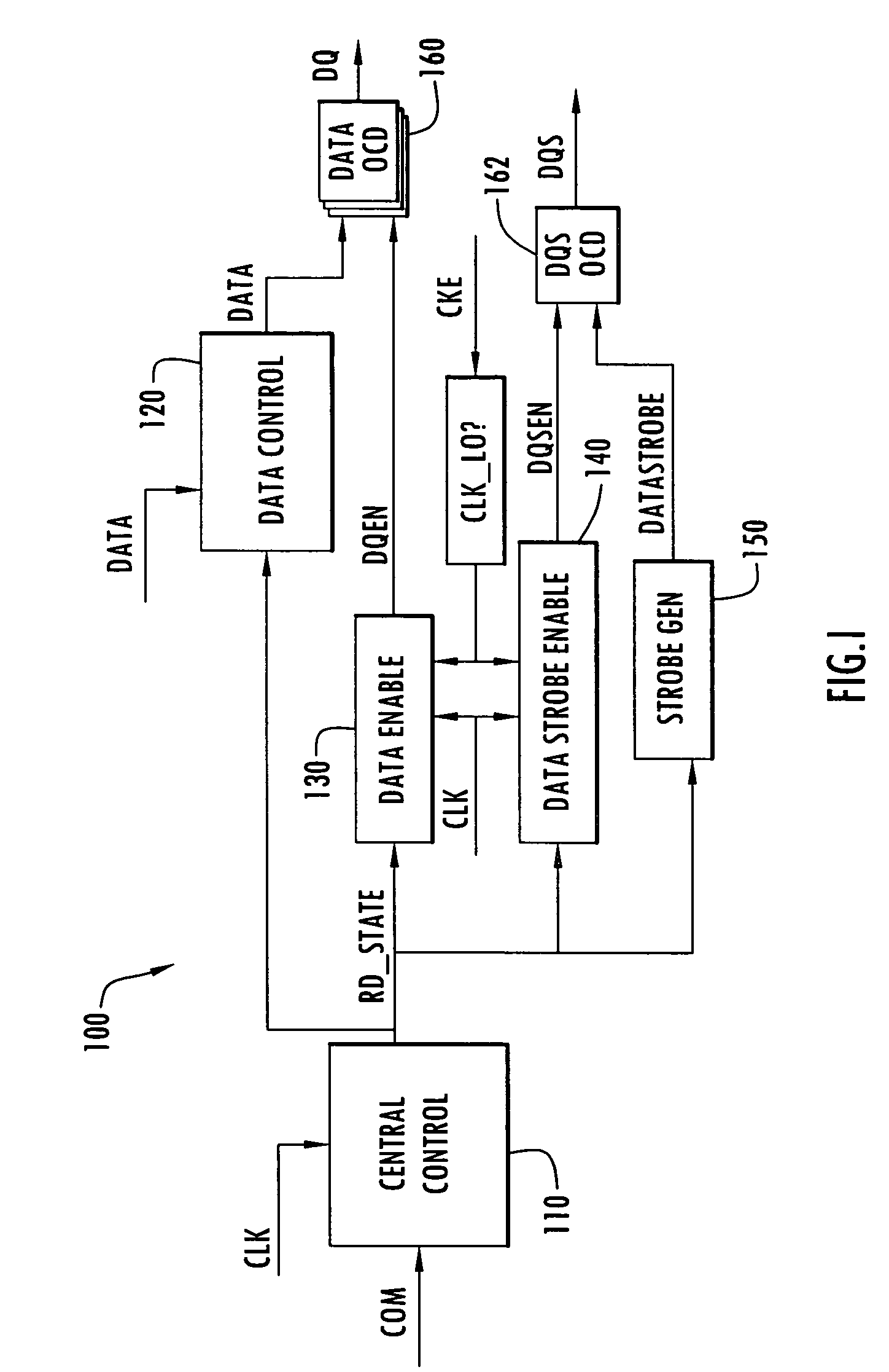
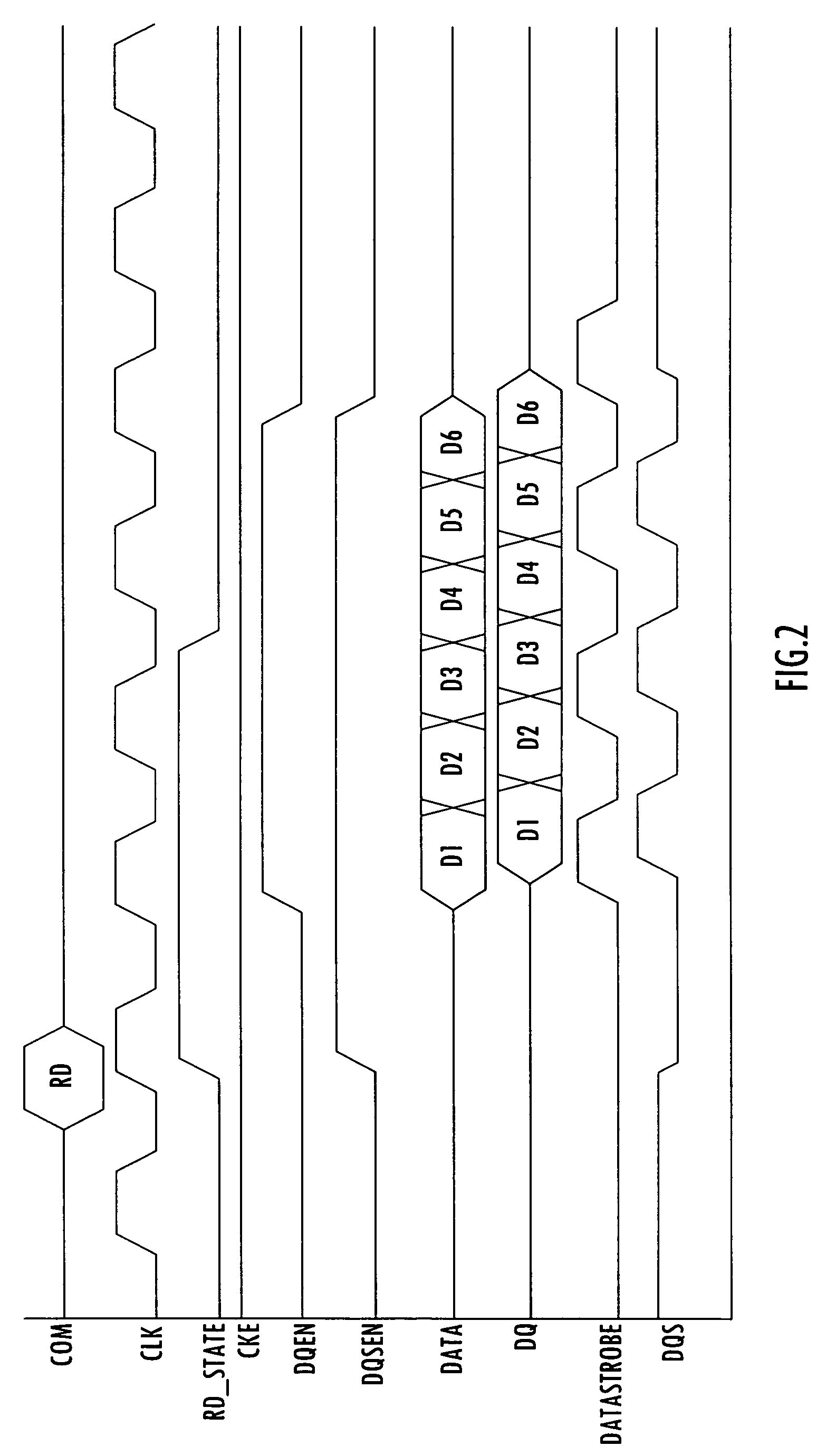
[0022]To better illustrate the invention, read burst and power down operations in a typical memory device will be described in connection with FIGS. 1–4 for contrast. More specifically, a block diagram of the read output section of a memory device 100 capable of implementing a power down read disable is shown in FIG. 1. Memory device 100 can be, for example, a DDR SDRAM chip capable of driving data off the chip at a double data rate (i.e., on both the rising and falling edges of a clock signal).
[0023]Included in memory device 100 is a central control module 110 which receives an external command signal (COM) and a clock signal (CLK). Central control module 110 supplies a read state signal (RD_STATE) to a data control module 120, a data enable module 130, a data strobe enable module 140, and a strobe generator block 150. A set of off-chip drivers (OCDs) 160 receives data from the data control module 120 and drives data (DQ) off the chip in accordance with a data enable signal (DQEN) ...
PUM
 Abstract
Description
Claims
Application Information


