Multi-chip package combining wire-bonding and flip-chip configuration

a multi-chip package and flip-chip technology, applied in the field of multi-chip package (mcp), can solve the problems of chip scale package not being reworked after molding, plurality of contact pads on the substrate for electrically connecting the chip scale package, and so as to reduce the warpage of the substrate 310

Active Publication Date: 2006-07-25
ADVANCED SEMICON ENG INC
View PDF6 Cites 69 Cited by
  • Summary
  • Abstract
  • Description
  • Claims
  • Application Information

AI Technical Summary

Benefits of technology

[0023]Referring to FIG. 7, another multi-chip package combining wire-bonding and flip-chip configuration is disclosed according to the forth embodiment of the present invention. The multi-chip package comprises some components, such as a substrate 310 with a plurality of contact pads, a molding compound 330 which seals wire-bonding chips and a flip-chip type electrical device 320, which are the same as the third embodiment of the

Problems solved by technology

In addition, the chip scale package is sealed inside the encapsulating material, so the chip scale package cannot be reworked after molding.
If the chip scale package is designed outside the encapsulating material, the plurality of contact pads on

Method used


Image

  • Multi-chip package combining wire-bonding and flip-chip configuration
  • Multi-chip package combining wire-bonding and flip-chip configuration
  • Multi-chip package combining wire-bonding and flip-chip configuration

Examples


first embodiment

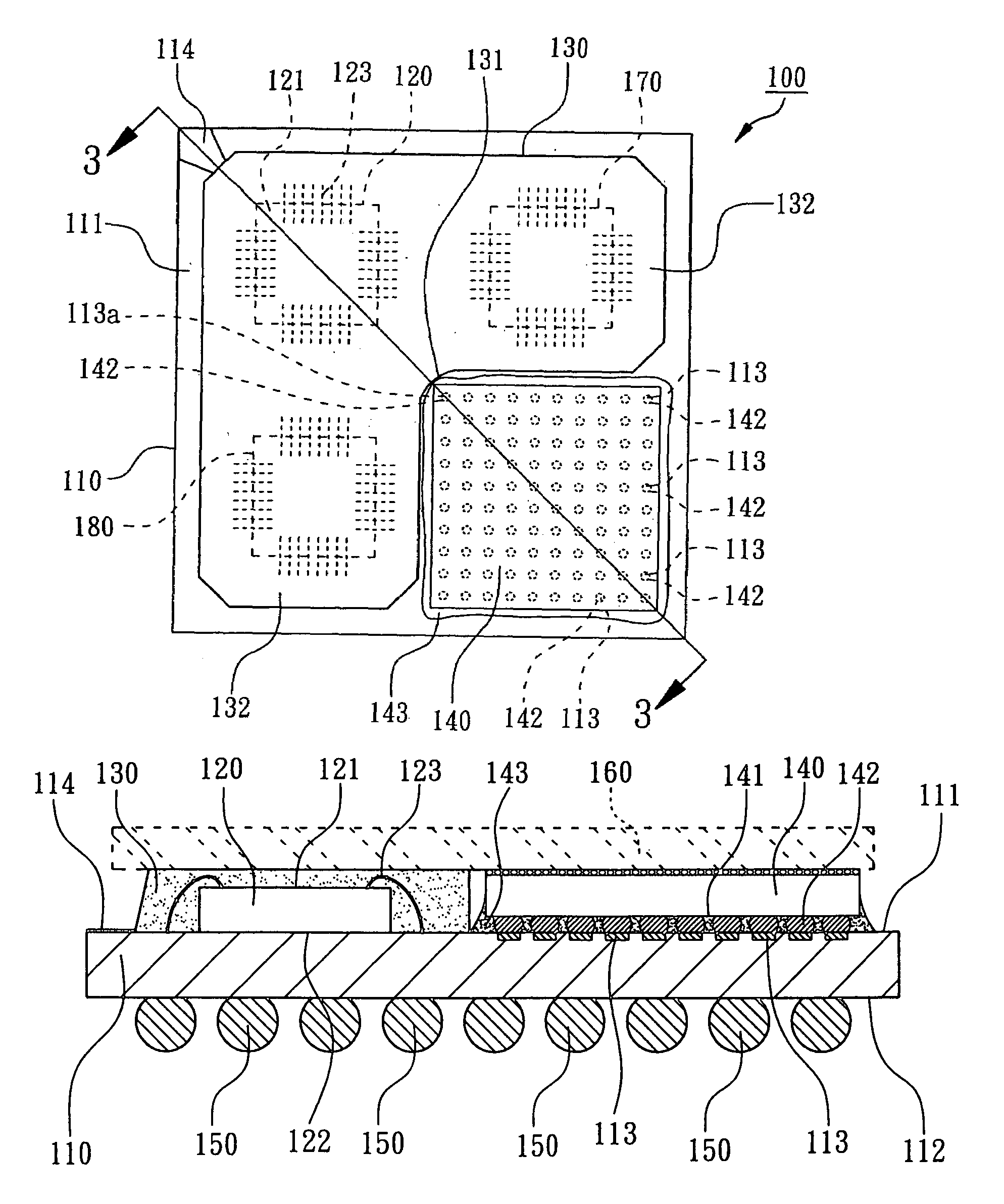
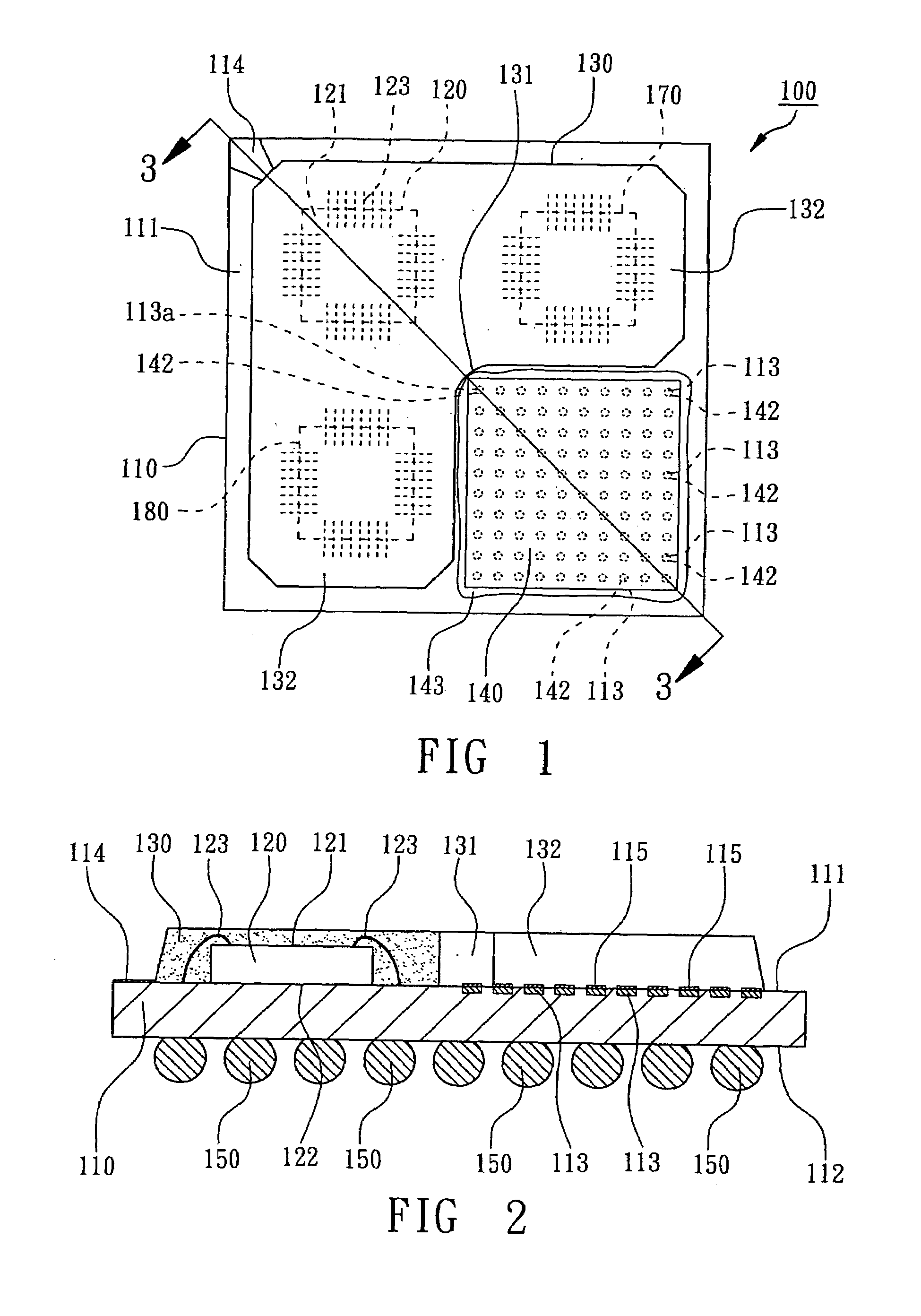
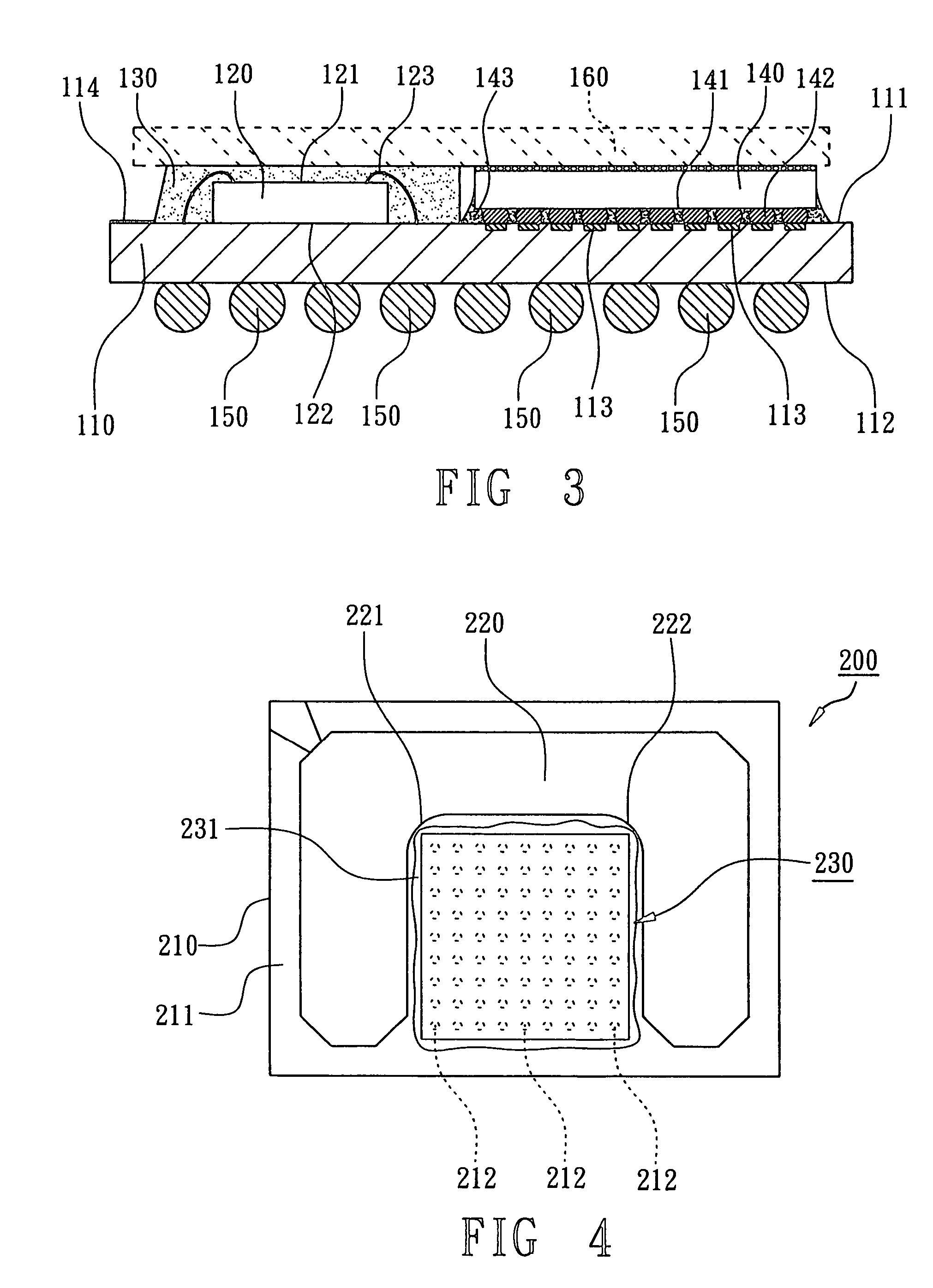
[0015]According to the present invention, a multi-chip package 100 combining wire-bonding and flip-chip configuration is showed in FIGS. 1, 2 and 3. FIG. 1 is a top view illustrating the multi-chip package 100. FIG. 2 is a cross-section view illustrating the multi-chip package 100 before mounting a flip-chip type electrical device 140. FIG. 3 is a cross-section view illustrating the multi-chip package 100 across I—I line of FIG. 1. The multi-chip package 100 comprises a substrate 110, at least a wire-bonding chip 120, a molding compound 130 and at least a flip-chip type electrical device 140.

[0016]Referring to FIGS. 1 and 3, the substrate 110, such as multi-layer printed circuit board or multi-layer ceramic substrate, has an upper surface 111 and a lower surface 112. A plurality of contact pads 113 are formed on the upper surface 111, and wiring traces electrically connect the upper surface 111 and the lower surface 112 (not show in the drawings). At least a wire-bonding chip 120 is...

second embodiment

[0021]Referring to FIG. 4, another multi-chip package 200 combining wire-bonding and flip-chip configuration is disclosed according to the present invention. The multi-chip package 200 comprises a substrate 210, a molding compound 220 and a flip-chip type electrical device 230. An upper surface 222 of the substrate 210 has a plurality of contact pads 212. The molding compound 220 formed by molding process seals at least an integrated circuit chip electrically connecting by wire bonding (not show in the drawing). The molding compound 220 partially covers the upper surface 211 of the substrate 210 but not covers the contact pads 212. In this embodiment, the molding compound 220 has a first recession 221, a second recession 222 and two symmetric extensions from the recession 221, 222. The molding compound 220 is in a U-shape to expose the contact pads 212 on the substrate 210. The recession 221, 222 are in a shape of an arc to keep a suitable distance from each recession 221, 222 to th...

third embodiment

[0023]Referring to FIG. 7, another multi-chip package combining wire-bonding and flip-chip configuration is disclosed according to the forth embodiment of the present invention. The multi-chip package comprises some components, such as a substrate 310 with a plurality of contact pads, a molding compound 330 which seals wire-bonding chips and a flip-chip type electrical device 320, which are the same as the present invention and use the same figure number. The molding compound 330 is selectively formed on the upper surface 311 of the substrate 310 by molding process. The molding compound 330 has a recession 331 and symmetric extensions 332 from two sides of the recession 331. The molding compound 330 forms an indentation 334 at the connecting portion of the symmetric extensions 332 to achieve reducing the warpage of the substrate 310.


PUM


Abstract

A multi-chip package combining wire-bonding and flip-chip configuration includes a plurality of chips, a substrate and a molding compound. Chip(s) with wire-bonding type and a flip-chip type electrical device are mounted on an upper surface of the substrate. A plurality of contact pads of the substrate are formed on the upper surface of the substrate that are not covered by the molding compound, so the flip-chip type electrical device can be electrically connected to these contact pads. The molding compound has recession(s) from a molding tool and seals the chip(s) with wire-bonding type without damaging the contact pads during molding process.

Description

FIELD OF THE INVENTION[0001]The present invention relates to a multi-chip package (MCP), and more particularly to a multi-chip package combining wire-bonding and flip-chip configuration.BACKGROUND OF THE INVENTION[0002]Based on the more request of the semiconductor package, a multi-chip package is developed for assembling a plurality of chips which having the same or different functions to make a system in package (SIP). According the different types of the chips, the multi-chip package assembles several kinds of chips by wire-bonding and flip-chip connection.[0003]R.O.C. Taiwan Patent No. 466719 entitled “multi chip module packaging method by mixing chip and package” disclosed a multi-chip module package. An encapsulating material on a substrate seals a wire-bonding chip and a chip scale package. The chip scale package is flip-chip mounted on the substrate, which includes a chip and a sub-package body. After mounting the chip scale package and the wire-bonding chip on the substrate...

Claims


Application Information

Patent Timeline
IPC IPC(8): H01L23/48H01L23/31H01L25/065
CPCH01L23/3121H01L25/0655H01L2224/48091H01L2224/48227H01L2224/73204H01L2224/16225H01L2224/73253H01L24/48H01L2224/16227H01L2924/15311H01L2924/00014H01L2224/05599H01L2224/45099H01L2224/85399H01L2924/14H01L2924/181H01L2224/83951H01L2224/73265H01L2224/45015H01L2924/207H01L2924/00H01L2924/00012
Inventor LIU, CHENG-CHENG
Owner ADVANCED SEMICON ENG INC
Why Eureka
Try Eureka