

Semiconductor laser device
a laser device and semiconductor technology, applied in semiconductor lasers, optical resonator shape and construction, instruments, etc., can solve the problems of high laser beam burden, complicated optical system, etc., and achieve low burden on solid-state laser medium, simple optical system, and easy maintenance of laser beam characteristics
- Summary
- Abstract
- Description
- Claims
- Application Information
AI Technical Summary
Benefits of technology
Problems solved by technology
Method used
Image

Examples
first embodiment
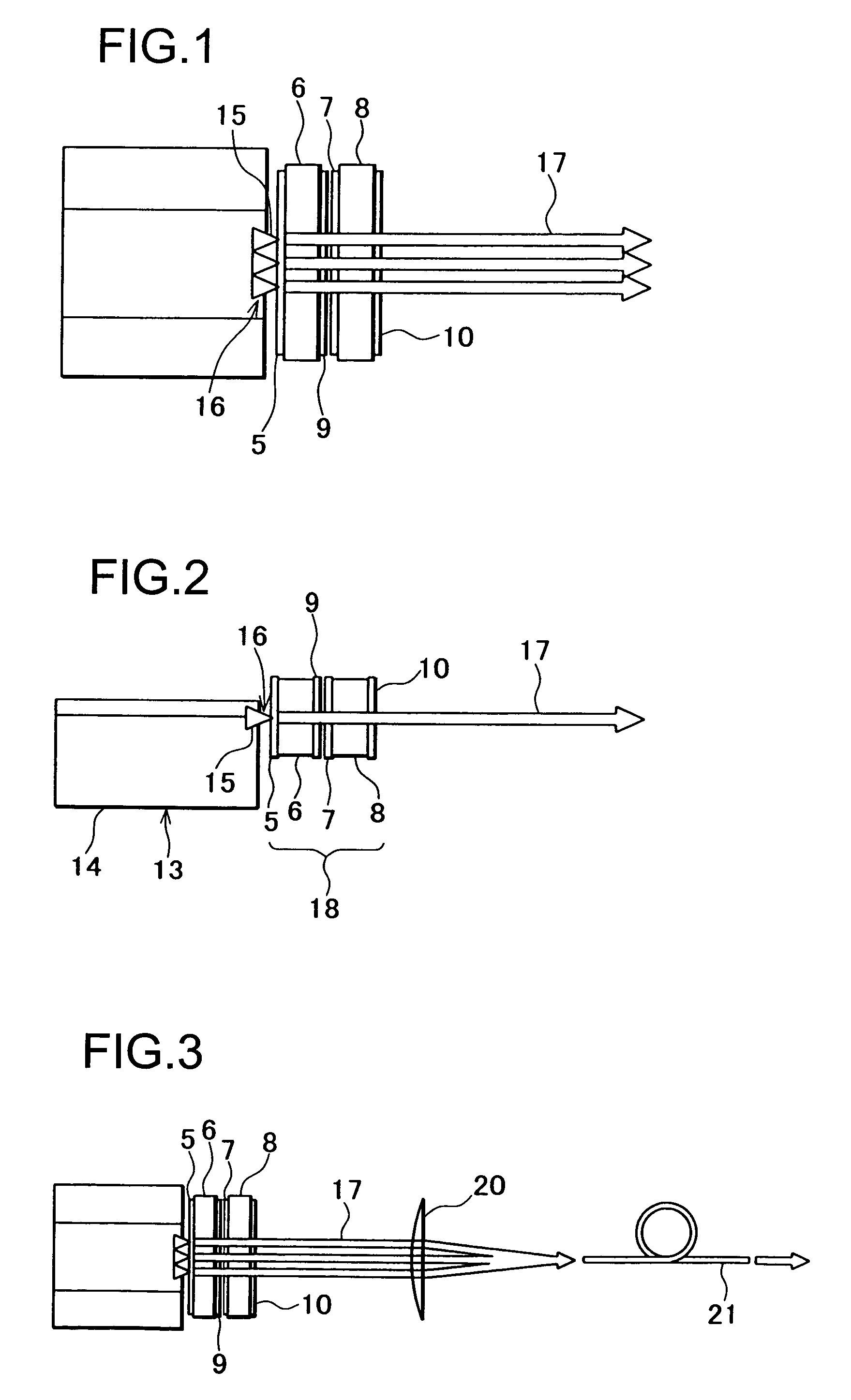
[0034]FIG. 1 and FIG. 2 each represents the present invention. In the figures, the same component as shown in FIG. 19 is referred by the same symbol.
[0035]A light emitter 13 comprises a light source retainer 14 with a flat upper surface, and as many semiconductor laser elements (semiconductor laser diodes (LDs)) 15 as required are arranged on the upper surface of the light source retainer 14. The semiconductor laser elements 15 are arranged in one row with a predetermined pitch to form a semiconductor laser element array 16.
[0036]A laser crystal plate (solid-state laser medium plate) 6 is arranged in proximity to the light source retainer 14 and in parallel to the semiconductor laser element array 16, and a transparent output reflection plate 8 is provided in parallel to the laser crystal plate 6.
[0037]On an end surface of the laser crystal plate 6 facing to the light emitter 13, there is a reflection mirror 5 which is a dielectric reflection film. On a surface of the output reflect...
second embodiment
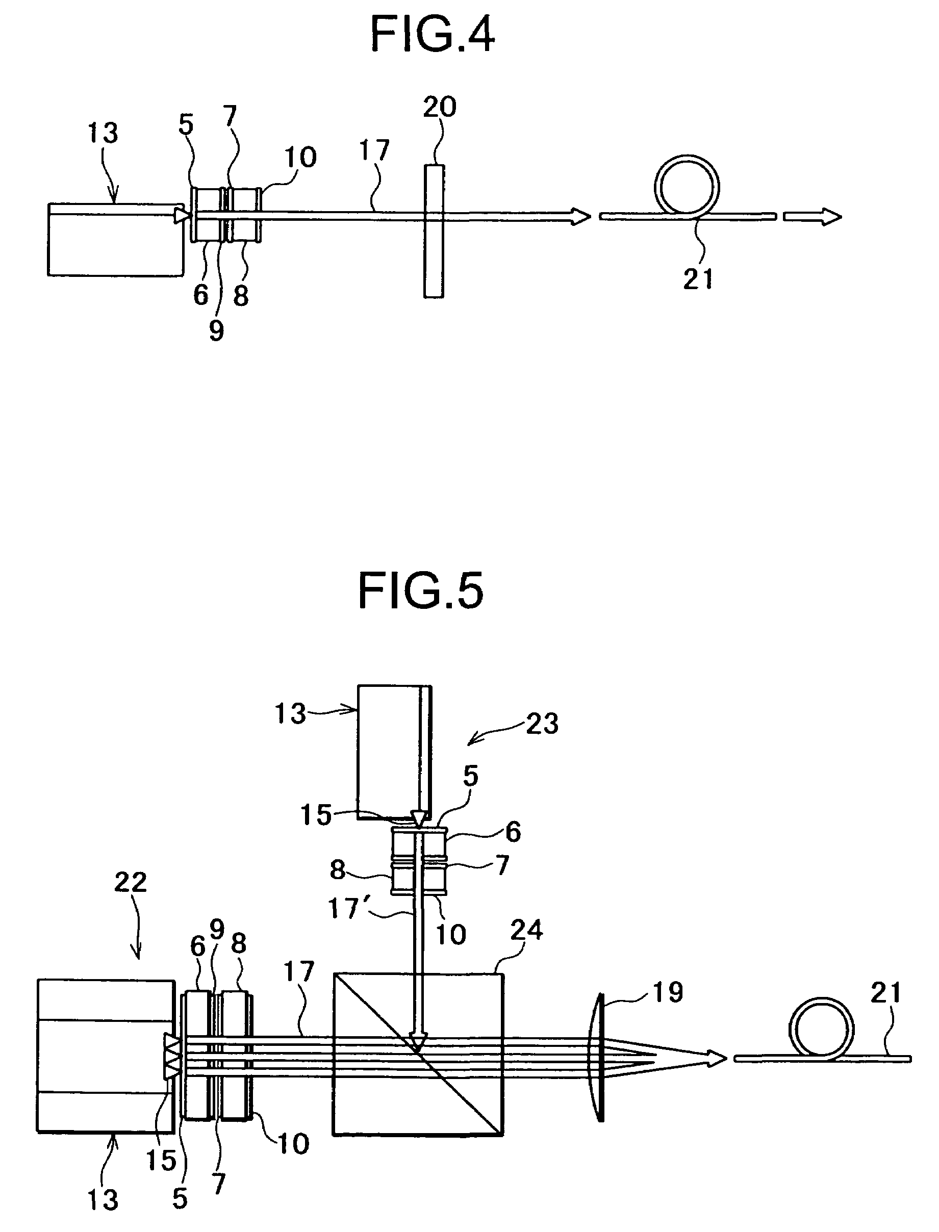
[0044]FIG. 3 and FIG. 4 each represents the present invention.
[0045]In the second embodiment, the laser beams 17 projected from the output reflection plate 8 are joined together through a cylindrical lens 20, and the laser beams are projected to a single optical fiber 21.
[0046]The laser beams 17 projected from the output reflection plate 8 are within the same plane and are running in parallel to each other. The cylindrical lens 20 is arranged to correspond to the output reflection plate 8, and an optical axis of the cylindrical lens 20 is made parallel to the laser beams 17. By the cylindrical lens 20, the laser beams 17 are joined at a single point. An end surface of the optical fiber 21 is positioned at a joining point of the laser beams 17, and all of the laser beams 17 emitted from the semiconductor laser elements 15 are projected to the optical fiber 21. From an other end of the optical fiber 21, all laser beams 17 joined together are irradiated. As an optical member to join th...
third embodiment
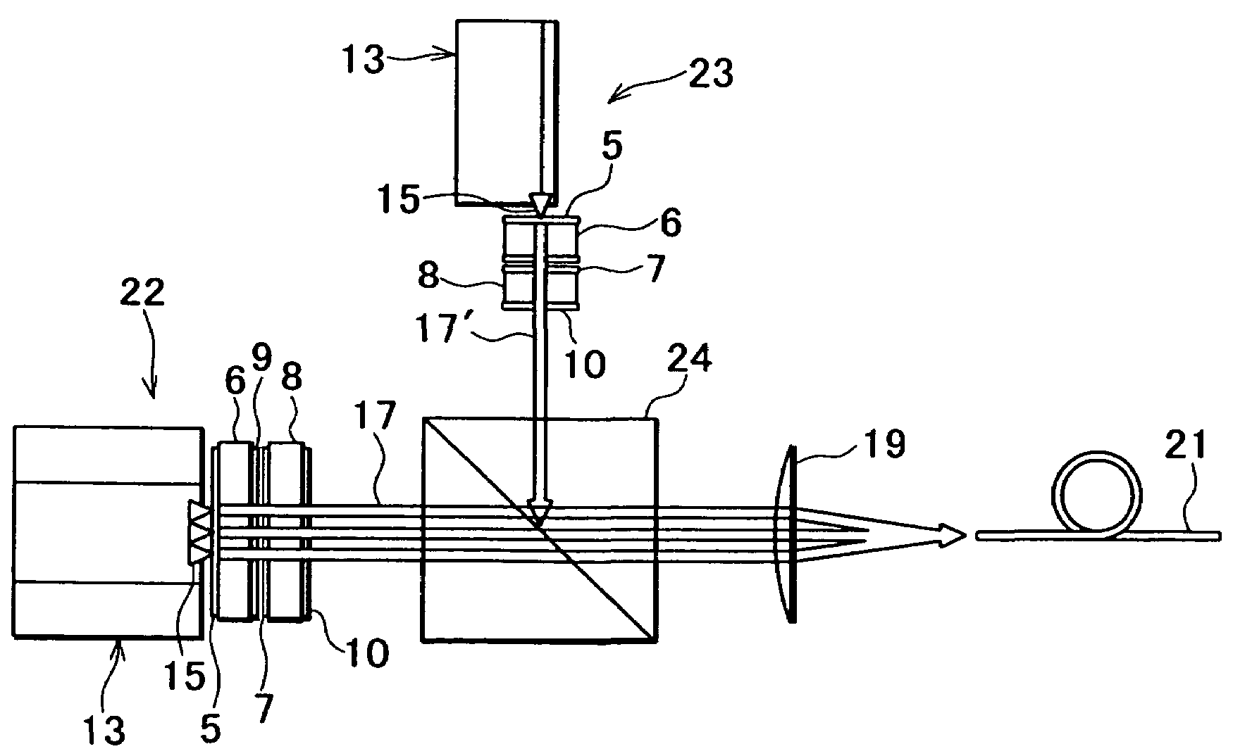
[0047]FIG. 5 shows the present invention.
[0048]In the third embodiment, two sets of the semiconductor laser devices as shown in the first embodiment are used as light emitting units 22 and 23.
[0049]In the light emitting units 22 and 23, as many semiconductor laser elements 15 as required are arranged on an upper surface of the light source retainer 14 and these elements make up together a light emitter 13. The semiconductor laser elements 15 are arranged in one row with a predetermined pitch and form a semiconductor laser element array 16. A laser crystal plate (solid-state laser medium plate) 6 is provided in parallel to the semiconductor laser element array 16. Further, an output reflection plate 8 is arranged in parallel to the laser crystal plate 6. On an end surface of the laser crystal plate 6 facing to the light emitter 13, a reflection mirror 5, i.e. a dielectric reflection film, is provided. On a surface of the output reflection plate 8 facing to the laser crystal plate 6, ...
PUM
 Abstract
Description
Claims
Application Information