Assembly of organic electroluminescence display device

a display device and organic technology, applied in the field of organic electroluminescence display devices, can solve the problems of increasing leakage current of organic el display devices, reducing durability and reliability, and complicated manufacturing process, so as to reduce internal optical loss, increase light bleeding efficiency, and increase the luminance of an image

Active Publication Date: 2006-08-01
SAMSUNG DISPLAY CO LTD
View PDF19 Cites 37 Cited by
  • Summary
  • Abstract
  • Description
  • Claims
  • Application Information

AI Technical Summary

Benefits of technology

[0019]The present invention provides an organic EL display device assembly which reduces internal optical loss and increases light bleeding efficiency to increase the luminance of an image.
[0020]The present invention also provides an organic El display device which reduces optical loss using a scattering efficiency at an interface between a layer with a high refractive index and a layer with a low refractive index.
[0021]According to an embodiment of the present invention, an organic electroluminescence (EL) display device assembly includes a substrate, an organic EL portion, an optical loss prevention layer, and a fine space layer. The organic EL portion has a first electrode layer, an organic luminescent layer, and a second electrode layer, which are each patterned and stacked on the upper surface of the substrate. The optical loss prevention layer increases light bleeding efficiency. The fine space layer is formed between the optical loss prevention layer and a layer facing the optical loss prevention layer and is filled with a gas or evacuated.
[0023]According to another embodiment of the present invention, an organic EL display device assembly includes a substrate, an organic EL display portion, a photonic plate, and a fine space layer. The organic EL display portion has a first electrode layer, an organic luminescent layer, and a second electrode layer, which are each patterned and stacked on the upper surface of the substrate. The photonic plate is combined with the organic EL display portion and has an optical loss prevention layer formed over the organic EL display portion. The fine space layer is formed between the optical loss prevention layer and the photonic plate and increases the light bleeding efficiency of light generated by the organic luminescent layer.

Problems solved by technology

Since this organic EL display device requires a wavy substrate, a wavy fine electrode pattern layer, or a special diffraction grating, its manufacturing process is complicated.
Thus, the leakage current of the organic EL display device increases and durability and reliability decrease.
However, since pixels depending on the luminescence of an organic film are very small, it is difficult to install the protrusion lens for condensing on the substrate.
In this organic EL display device, since the luminescent layer is very thin, it is very difficult to install a reflective mirror on one side of the luminescent layer.
In this organic EL display device, since reflected light bleeds toward the glass substrate, the bleeding efficiency increases, but images become blurred.

Method used


Image

  • Assembly of organic electroluminescence display device
  • Assembly of organic electroluminescence display device
  • Assembly of organic electroluminescence display device

Examples


first experiment

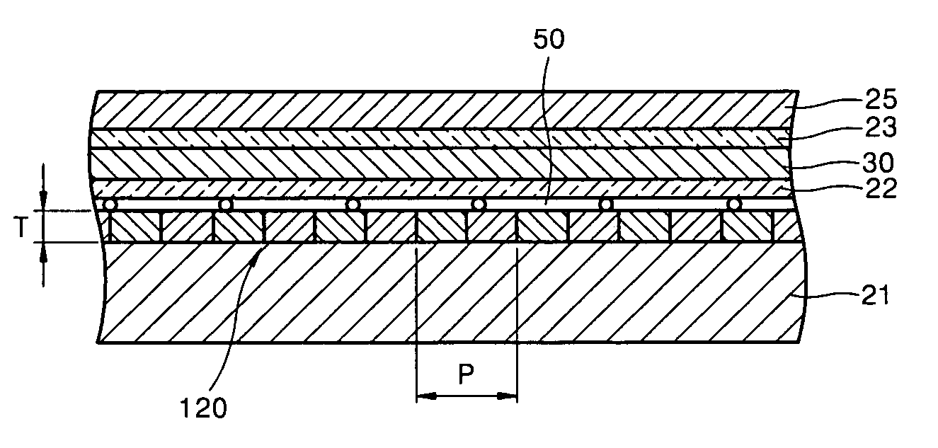
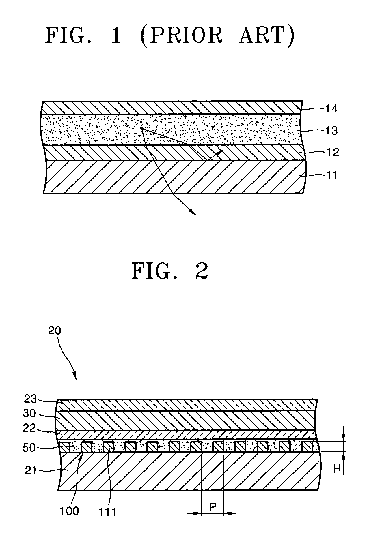
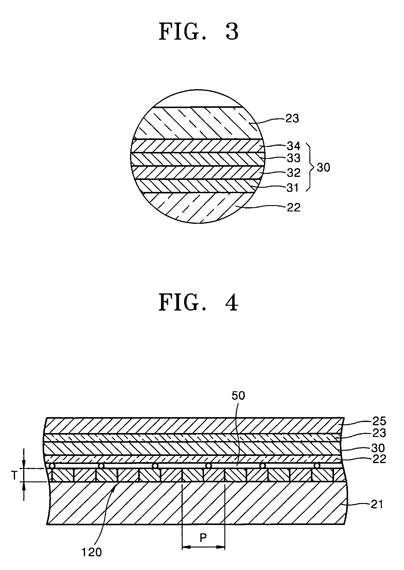
[0066]The first experiment was performed on an organic EL display device in which an optical loss prevention layer having cylindrical protrusions was formed of SiO2, TiO2, and SiNx on the upper surface of a substrate. The pitch between adjacent protrusions was in the range of 200 nm to 2000 nm, and the height of each of the protrusions was in the range of 50 nm to 5000 nm.

[0067]A first electrode layer, an organic luminescent layer, and a second electrode layer were sequentially stacked on the upper surface of the resulting substrate and between the resulting substrate and a fine space layer. FIG. 13 is a graph of a measured optical efficiency versus the width of the gap of the fine space layer. FIG. 14 is a graph of optical efficiency versus the height of the cylindrical protrusions.

[0068]Through the first experiment, standardized optical energy values were calculated for different widths of the gap of the fine space layer using a Finite Difference Time Domain (FDTD) simulation. In ...

second experiment

[0072]The second experiment was performed on an organic EL display device in which an index layer was formed of TiO2 with a refractive index of 2.36 between the fine space layer and the first electrode layer under the same conditions as in the first experiment. FIG. 15 is a graph of optical efficiency versus the thickness of the index layer. Here, the gap of the fine space layer was 0, and the protrusions of the optical loss prevention layer were 400 nm high.

[0073]According to FIG. 15, when the thickness of the index layer was 50 nm, the optical efficiency increased by about 4 times and the amount of light bleeding increased by 47.1% compared to the organic EL display device of the first comparative experiment.


PUM


Abstract

An organic electroluminescence (EL) display device assembly includes a substrate, an organic EL portion, an optical loss prevention layer, and a fine space layer. The organic EL portion has a first electrode layer, an organic luminescent layer, and a second electrode layer which are each patterned and stacked on the upper surface of the substrate. The optical loss prevention layer is used to increase light bleeding efficiency. The fine space layer is formed between the optical loss prevention layer and a layer facing the optical loss prevention layer and is filled with a gas or evacuated.

Description

CROSS-REFERENCE TO RELATED APPLICATIONS[0001]This application claims the benefit of Korean Application No. 2003-14000, filed Mar. 6, 2003, in the Korean Intellectual Property Office, the disclosure of which is incorporated herein by reference.BACKGROUND OF THE INVENTION[0002]1. Field of the Invention[0003]The present invention relates to organic electroluminescence (EL) display devices, and more particularly, to an organic EL display device with improved light bleeding efficiency of light emitted from an organic film.[0004]2. Description of the Related Art[0005]Organic EL display devices are spontaneous light-emitting display devices that emit light by electrically exciting a fluorescent organic compound. Typically, organic EL display devices may operate at a low voltage, be formed compactly to form a thin device, and provide a wide viewing angle and a high response speed. Organic EL display devices are the focus of considerable attention because they may be used as next-generation ...

Claims


Application Information

Patent Timeline
Patent Type & Authority Patents(United States)
IPC IPC(8): H05B33/22H05B33/02G09F9/30H01L27/32H01L51/50H01L51/52H05B33/00H05B33/14
CPCH01L51/5262H01L27/3244H01L2251/5315H10K59/12H10K50/85H10K2102/3026H05B33/22
Inventor CHO, SANG-HWANDO, YOUNG-RAGKIM, YOON-CHANGAHN, JI-HOONLEE, JOON-GU
Owner SAMSUNG DISPLAY CO LTD
Why Eureka
Try Eureka