
Distributed random access memory in a programmable logic device

a random access memory and programmable logic technology, applied in the direction of computation using denominational number representation, pulse technique, instruments, etc., can solve the problems of increasing the number of logic elements that can be made available, limiting user flexibility, and increasing the cost. cost

Active Publication Date: 2006-08-01
ALTERA CORP
View PDF18 Cites 27 Cited by
  • Summary
  • Abstract
  • Description
  • Claims
  • Application Information

AI Technical Summary

Benefits of technology

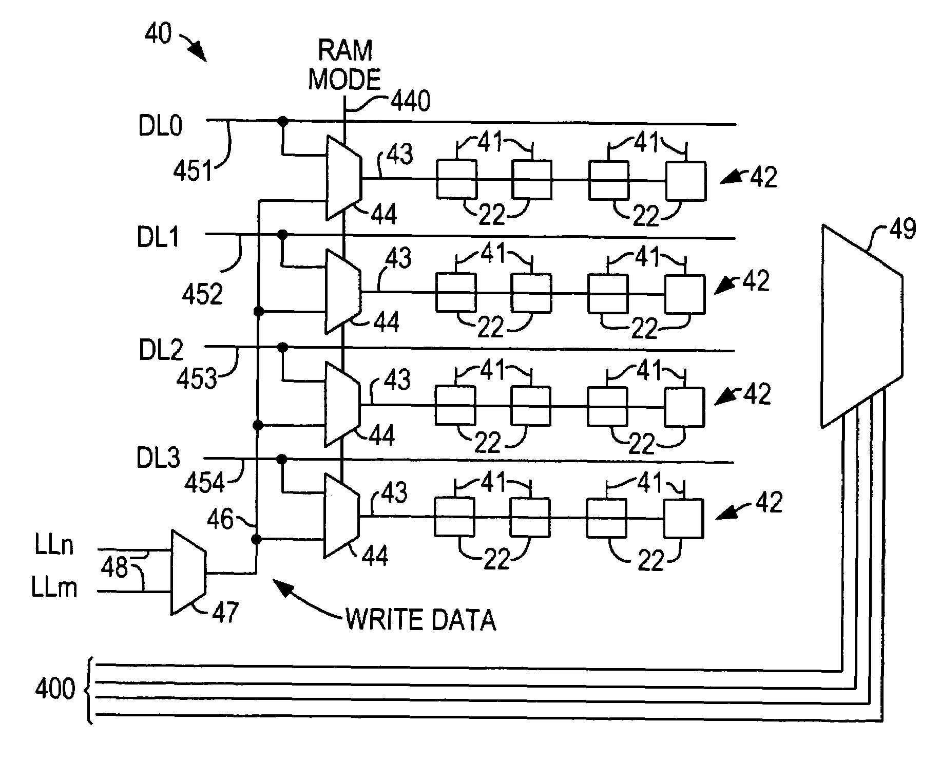
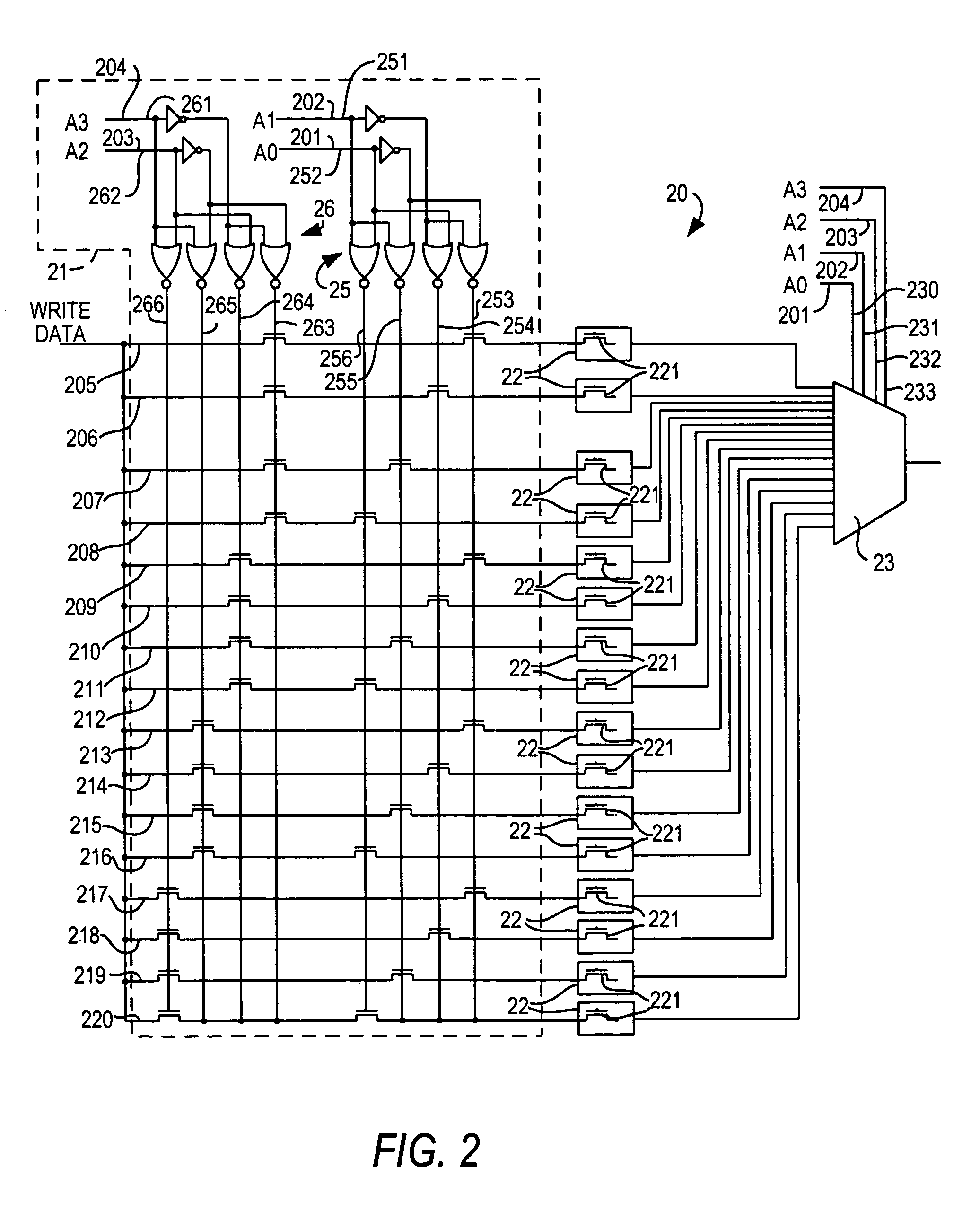
[0005]The present invention provides distributed RAM at lower cost by sharing the signal path for writing data into the distributed RAM as well as for configuration of the PLD. This is combined with a decoder which can be amortized over a plurality of logic elements, and therefore requires fewer additional transistors or switches in the individual logic elements.
[0006]As discussed in more detail below, a number of variations of decoder and signal path combinations according to the present invention are possible, providing different tradeoffs of speed and area. Moreover, the invention uses a lower cost write data path when such a path is necessary, allowing all bits of RAM to be used as distributed RAM.

Problems solved by technology

As more transistors and signal paths are added to accommodate the distributed RAM, additional area is required and the cost increases, or alternatively the number of logic elements that can be made available for inclusion in distributed RAM must be limited, which limits user flexibility.

Method used


Image

  • Distributed random access memory in a programmable logic device
  • Distributed random access memory in a programmable logic device
  • Distributed random access memory in a programmable logic device

Examples


Embodiment Construction

[0038]The invention will now be described with reference to FIGS. 1–26.

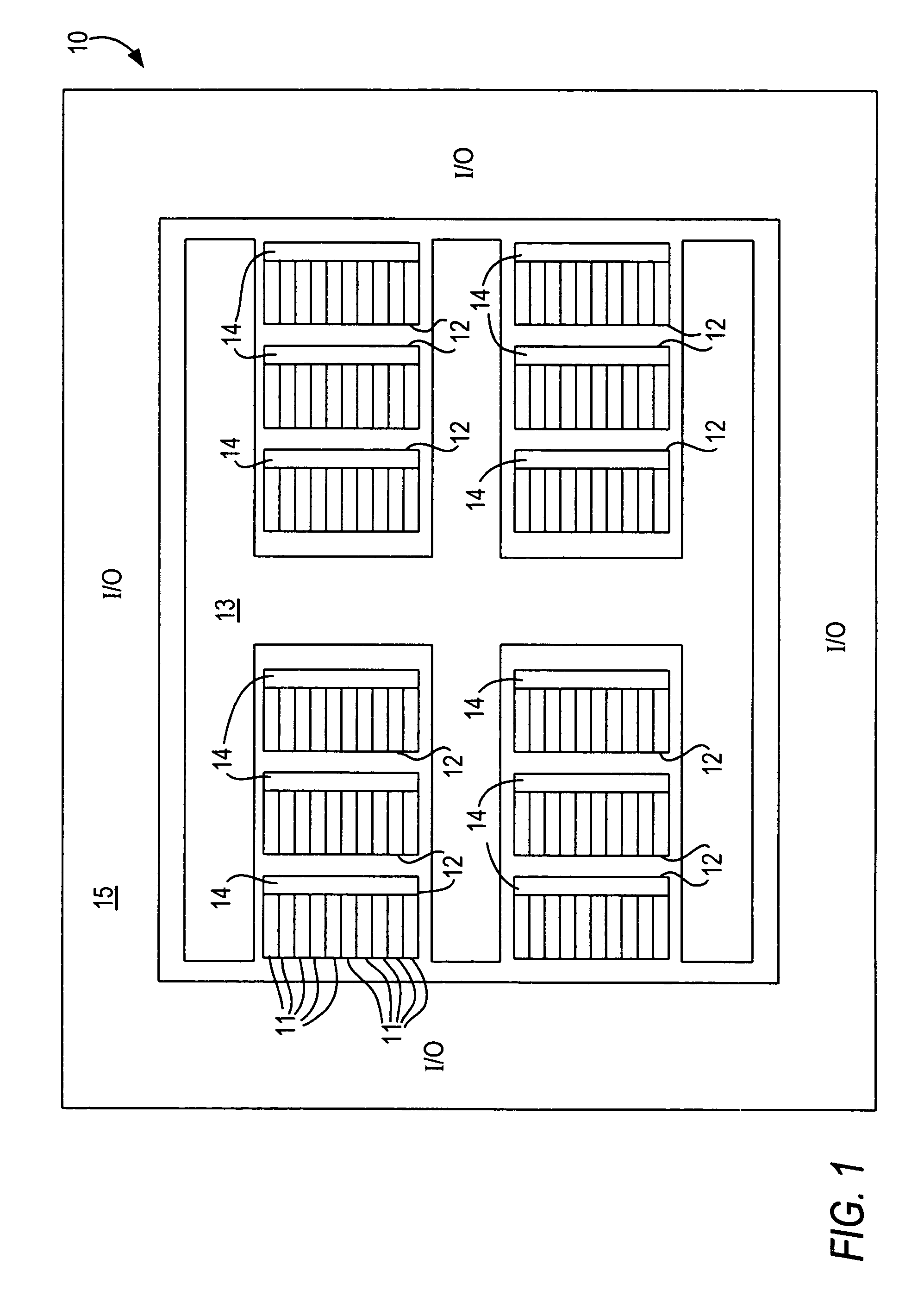
[0039]FIG. 1 shows a representation of a PLD 10 that may incorporate the invention. PLD 10 includes a plurality of logic cells or elements (LEs) 11, arranged in groups or “logic array blocks (LABs)”12, interconnected by routing shown generally at 13. Routing, shown schematically at 14 also exists inside LABs 12 to interconnect LEs 11. As described above, each LE 11 includes a plurality of RAM bits used for configuration. A typical LE may be configured as a four-input look-up table, having sixteen configuration bits. Input / output regions 15 preferably are located adjacent the edges of PLD 10.

[0040]PLD 10 may optionally include blocks of RAM (not shown). Whether or not such blocks are present, it may be desirable to use some or all of the configuration bits as distributed user RAM (or read-only memory (ROM)). A typical LE normally already includes the necessary circuitry for reading as distributed RAM. For example,...


PUM


Abstract

Distributed random access memory in a programmable logic device uses configuration RAM bits as bits of the distributed RAM. A single write path is used to provide both configuration data and user write data. Selection circuitry, such as a multiplexer, is used to determine whether the single write path carries configuration data or user write data. In another aspect of the invention, the configuration RAM bits are used as to construct a shift register by adding pass transistors to chain the configuration RAM bits together, and clocking alternate pass transistors with two clocks 180° out of phase with one another.

Description

BACKGROUND OF THE INVENTION[0001]This invention relates to using the configuration bits of a programmable logic device as distributed random access memory (“RAM”). More particularly, this invention relates to reducing the costs of circuitry needed to implement distributed RAM in a programmable logic device.[0002]A common type of programmable logic device (“PLD”) in use today uses static RAM bits to configure programmable logic components to implement a user logic design. It is known to provide circuitry in a PLD to allow a user to configure those configuration bits in otherwise unused portions of the PLD to function as RAM. For example, in some user designs, it may be more advantageous to use unused configuration bits as RAM rather than using a separate RAM device, because the amount of RAM needed is small, or because using on-chip RAM is faster. A RAM formed from such distributed configuration bits may be referred to as “distributed RAM.”[0003]Contemporary PLDs are typically organi...

Claims


Application Information

Patent Timeline
IPC IPC(8): H03K19/177
CPCH03K19/1776H03K19/17736
Inventor LEWIS, DAVIDLEVENTIS, PAULBETZ, VAUGHN
Owner ALTERA CORP
Learn More