Optical head and optical device for enhancing the intensity of a transmitted light

Inactive Publication Date: 2006-08-01
NEC CORP
View PDF9 Cites 22 Cited by
  • Summary
  • Abstract
  • Description
  • Claims
  • Application Information

AI Technical Summary

Benefits of technology

[0013]A first object of the present invention is to provide an optical device having a high efficiency of the transmission light to the incident light. And a first aspect of the present invention is an optical device including conductive films having first and second surfaces, at least one hole perforated from said first surface to said second surface, and surface specific shapes periodically provided on at least one of the first and second surfaces in which a light incident upon the one surface enhances an intensity transmitted through the hole, wherein the conductive films are of a multilayered structure having an intermediate layer between said first and second surfaces. In the present invention, the multilayered structure may be comprised of single conductive film and the intermediate layer. In this case,

Problems solved by technology

Such optical disc generally shows significant disadvantages when the read speed (the speed of data which can be read from the optical disc) is relatively low.
When using such a small hole, the transmission through the hole in a prior art optical device using a near field, such as a tapered front edge of an optical fiber, is susceptible to severe attenuation.
The signal-to-noise ratio is too low for reading and a sufficient optical intensity needed for writing cannot be obtained.
A practical optical data read / write head using a near field optical system has not been obtained.
The sub-wavelength hole device showing a sufficient transmission efficiency has not been realized.
In the high efficiency optical transmission using the surface plasmon shown by Ebbesen et al., a sufficient optical transmission efficiency has not been obtained yet in the prior art manufacturing method.
As described above, the read / write head for an optical data recording medium of an optical device using a near field optical system is not practical.
But, in this case, it is a problem that the efficiency of the transmission light to the incident light is not sufficient.

Method used


Image

  • Optical head and optical device for enhancing the intensity of a transmitted light
  • Optical head and optical device for enhancing the intensity of a transmitted light
  • Optical head and optical device for enhancing the intensity of a transmitted light

Examples


Embodiment Construction

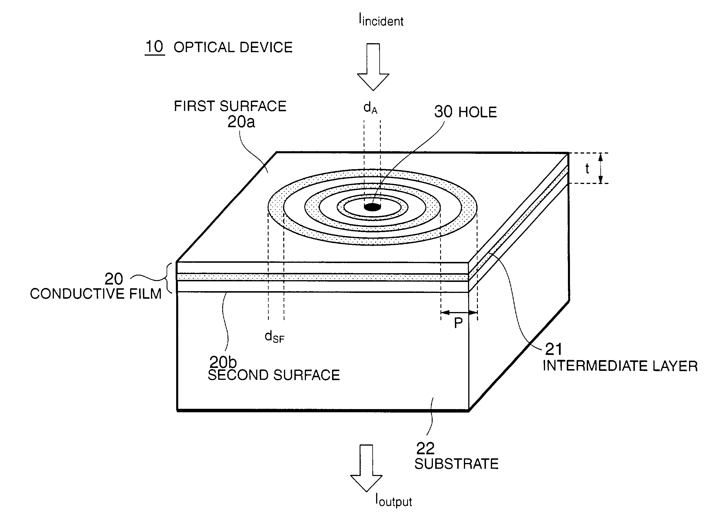
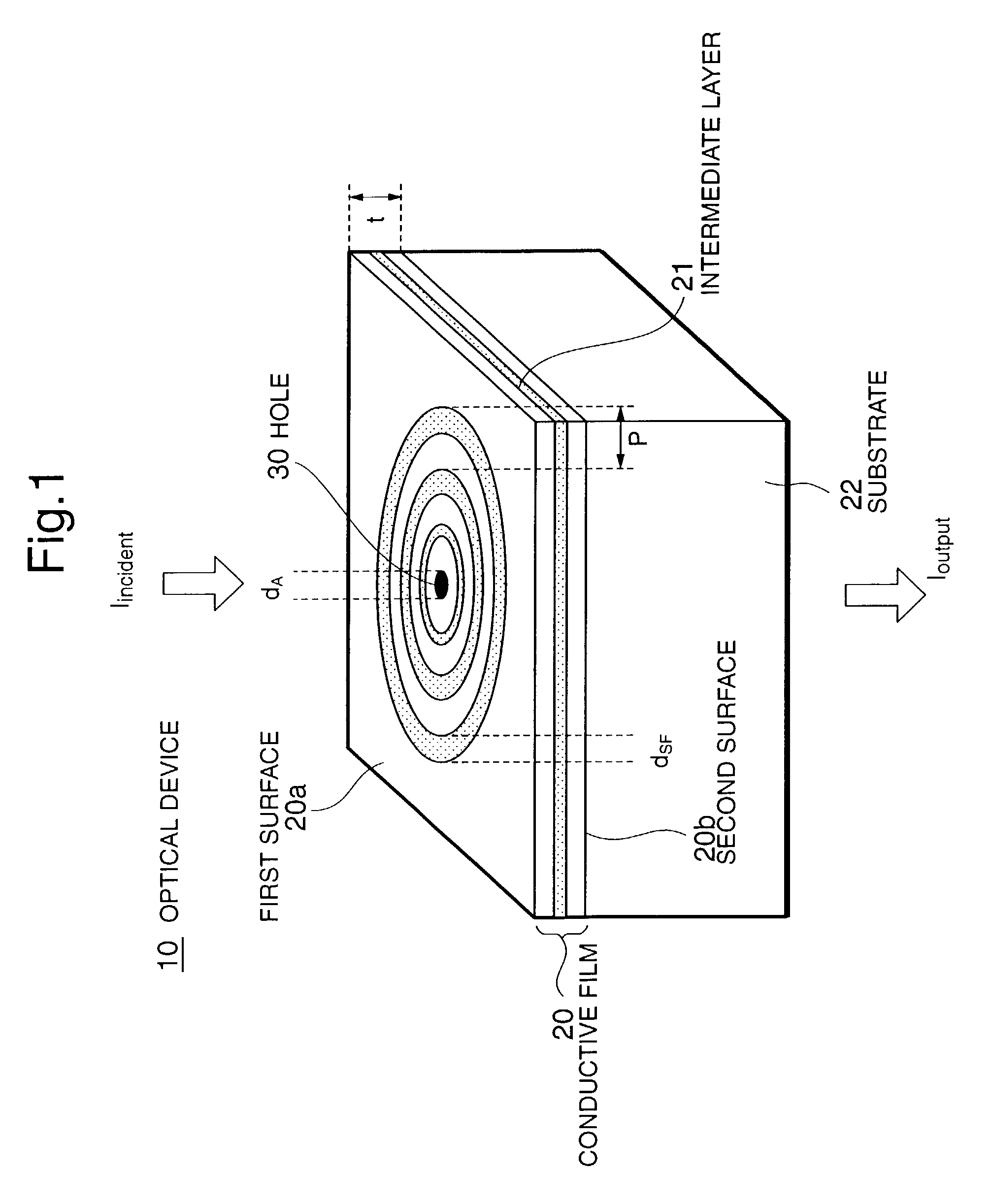
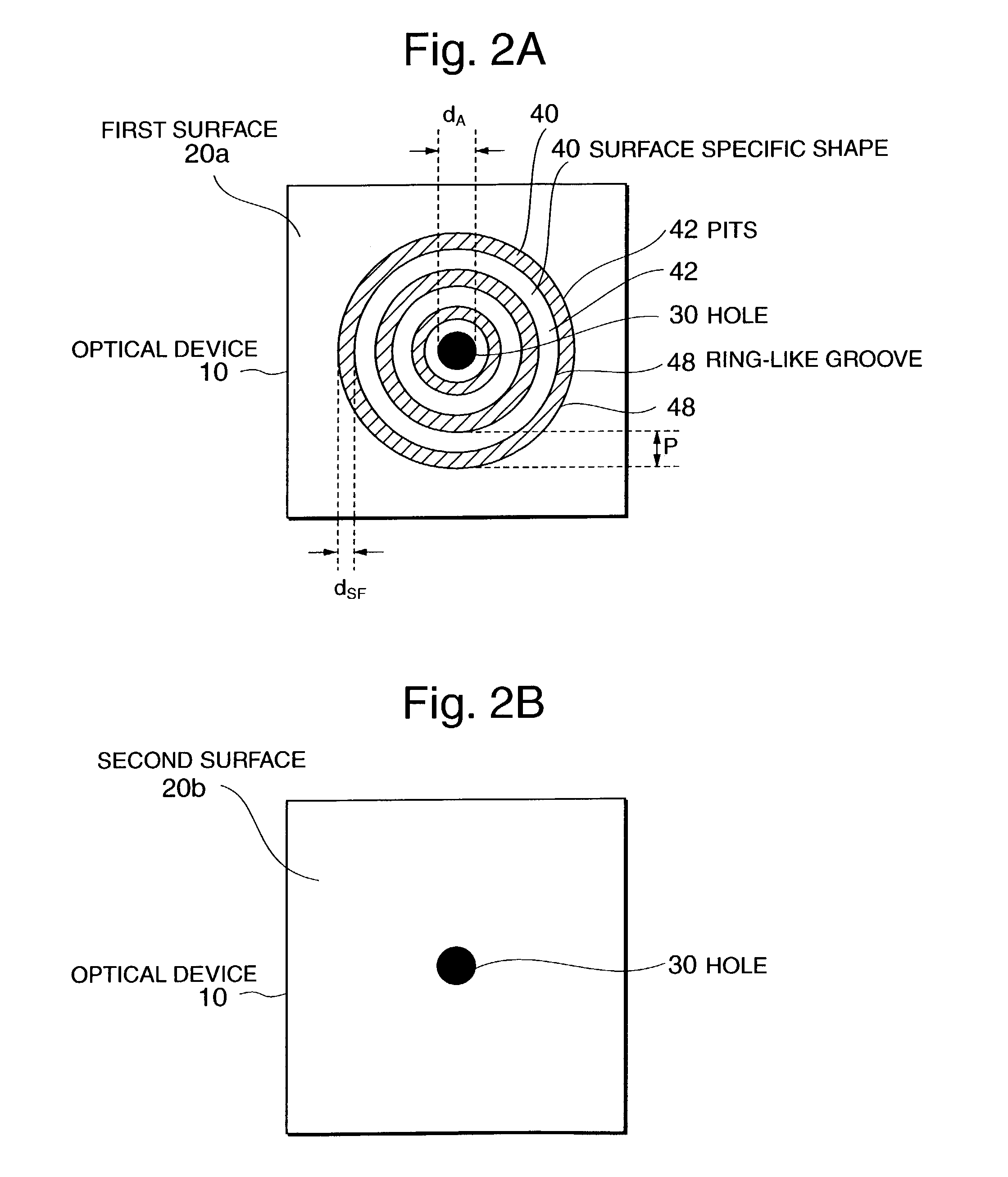
[0028]Preferred embodiments of the present invention will be discussed in detail with reference to the drawings.

[0029]Before explaining the specific embodiments of the present invention, some conditions will be described to understand the present invention.

[0030]The material forming a layer having a first surface of a conductive film and a layer having a second surface thereof is a conductive material such as all metals and a doped semiconductor. Aluminum, silver, gold or chrome is preferable.

[0031]The surface refers to an almost flat surface and all surfaces including surface shapes showing regions swelled or depressed periodically unlike the same. The regions of the surface shapes are arrayed in a periodic or regular repetitive pattern (for example, a regular two-dimensional lattice).

[0032]A hole passes through all thicknesses of the conductive films. The conductive film is nominally flat except for the hole. To identify projections and pits, the projections and pits of the surfac...


PUM


Abstract

A optical device including conductive films having a first and second surfaces, one hole, surface specific shapes periodically, and a layer inserted as an intermediate layer between the first and the second surface of conductive films. The intermediate layer has the effect for improving surface roughness of the surface of conductive film. A light incident upon one surface enhances an intensity transmitted though the hole.

Description

BACKGROUND OF INVENTION[0001]1. Field of the Invention[0002]The present invention relates to an optical device and an optical head using the same. More specifically, the present invention relates to an optical device having a very high throughput and resolution using surface-plasmon-enhanced optical transmission through a sub-wavelength hole in conductive films and a head for an optical recording medium using the same.[0003]2. Description of the Related Art[0004]An optical recording disc such as a CD (compact disc) and DVD (digital video disc) is an increasingly attractive data recording medium because of its high data recording density, compact design, portability, robustness and the lower costs of both the medium and a write device. Irrespective of a relatively high data density provided by the optical disc, a higher recording density is thought to be desirable. A smaller spot provides a higher data recording density on the optical recording medium and a higher data read speed to ...

Claims


Application Information

Patent Timeline
IPC IPC(8): G11B7/00G02B6/42G11B7/135G11B7/1387
CPCG11B7/1387B82Y10/00
Inventor FUJIKATA, JUNICHIYOKOTA, HITOSHIISHI, TSUTOMU
Owner NEC CORP
Why Eureka
Try Eureka