Textured substrate tape and devices thereof
a technology of textured substrates and tapes, applied in the direction of superconductor devices, polycrystalline material growth, transportation and packaging, etc., can solve the problem of undesirable high angle grain boundaries of substrates
- Summary
- Abstract
- Description
- Claims
- Application Information
AI Technical Summary
Benefits of technology
Problems solved by technology
Method used
Image

Examples
example 1
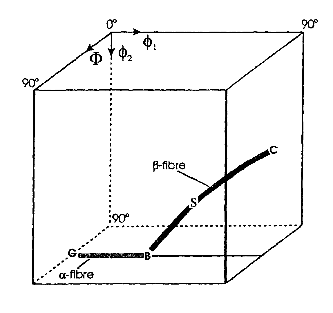
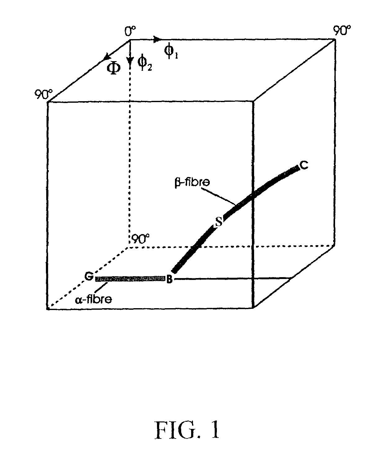
[0087]Ni was heavily deformed at about 10% reduction per pass starting from a thick slab of 1″ to 125 microns thick tape. The tape was rolled by reverse rolling in each pass. X-ray diffraction of the as-deformed tape indicated the formation of an ideal Cu-type texture [11].
[0088]For such a deformed tape, it is well established that much of the intensity lies along the β-fiber. This material starts to undergo primary recrystallization at about 400° C. It further undergoes secondary recrystallization at temperature greater than 1200° C. Sample of as-deformed Ni were placed in a furnace at room temperature in flowing 4% H2-96%-Ar. The furnace was quickly heated to 1300° C. and the sample held for one hour at that temperature. The sample was then furnace cooled to room temperature.
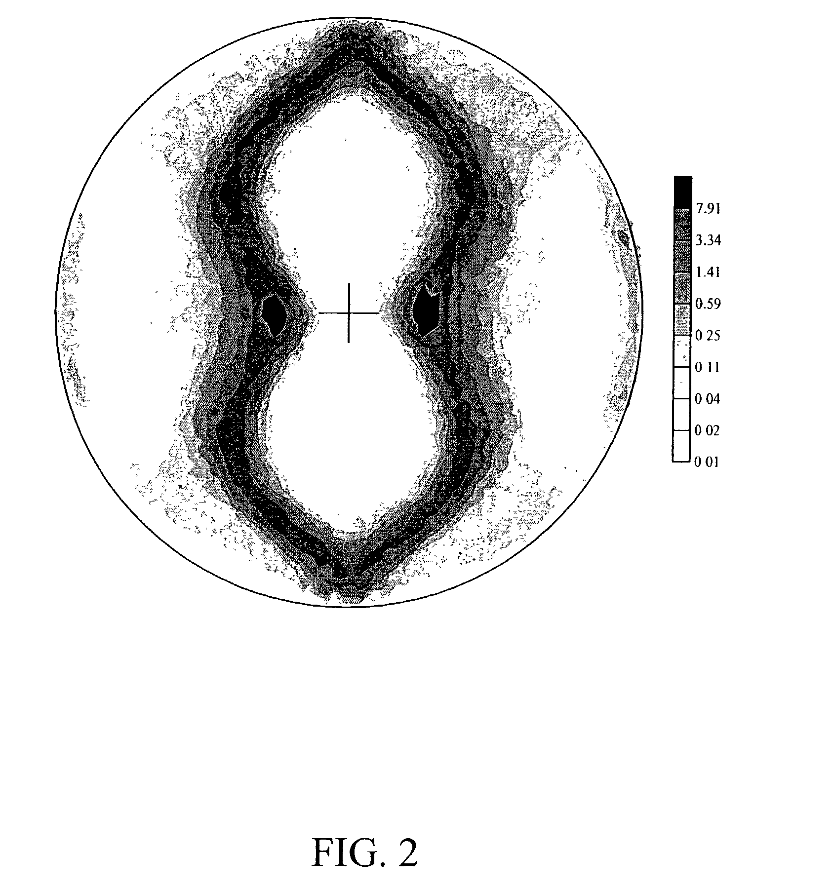
[0089]FIGS. 8(a) and 8(b) show (200) and (111) pole figure of Ni single crystal substrate fabricated by secondary recrystallization, respectively. It can be seen that [002] axis of the Ni tape is rotated with ...
example 2
[0093]A Ni—Cr alloy with 13 at % Cr was cold rolled to form a well developed Cu-type rolling texture. The sample was found to have a secondary recrystallization temperature of 1050° C. The Ni—Cr sample was annealed in 4% H2-96% Ar for one hour at 1300° C. The sample was then furnace cooled. It was found that the substrate was essentially a single crystal with a texture similar to that shown in FIGS. 8(a) and (b). The surface of the crystal was adequately sulfurized to form a c(2×2) sulfur superstructure [13]. Epitaxial oxide buffer layers and a superconductor layer were deposited on the substrate according to conditions shown in Example 1 to yield a high-Jc material. Deposition of an epitaxial Ni buffer layer before the deposition of any other oxide buffer layer was found to be easier to work with.
example 3
[0094]A Ni—W alloy with 5 at % W was cold rolled to form a well developed Cu-type rolling texture. The sample was found to have a secondary recrystallization temperature of 1050° C. The Ni—W sample was annealed in 4% H2-96% Ar for one hour at 1300° C. The sample was then furnace cooled. It was found that the substrate was essentially a single crystal with a texture similar to that shown in FIGS. 8(a) and (b). The surface of the crystal was adequately sulfurized to form a c(2×2) sulfur superstructure [13]. Epitaxial oxide buffer layers and a superconductor layer were deposited on the substrate according to conditions shown in Example 1 to yield a high-Jc material. Deposition of an epitaxial Ni buffer layer before the deposition of any other oxide buffer layer was found to be easier to work with.
PUM
| Property | Measurement | Unit |
|---|---|---|
| Length | aaaaa | aaaaa |
| Length | aaaaa | aaaaa |
| Length | aaaaa | aaaaa |
Abstract
Description
Claims
Application Information
 - R&D
- Intellectual Property
- Life Sciences
- Materials
- Tech Scout
- Unparalleled Data Quality
- Higher Quality Content
- 60% Fewer Hallucinations
Browse by: Latest US Patents, China's latest patents, Technical Efficacy Thesaurus, Application Domain, Technology Topic, Popular Technical Reports.
© 2025 PatSnap. All rights reserved.Legal|Privacy policy|Modern Slavery Act Transparency Statement|Sitemap|About US| Contact US: help@patsnap.com