Process for the formation of a spatial chip arrangement and spatial chip arrangement

Inactive Publication Date: 2006-08-08
PAC TECH PACKAGING TECH
View PDF56 Cites 11 Cited by
  • Summary
  • Abstract
  • Description
  • Claims
  • Application Information

AI Technical Summary

Benefits of technology

[0004]The object underlying the present invention is therefore to propose a process for the formation of a spatial chip arrangement despite the fact that a high integration density

Problems solved by technology

By reason of the high integration density—that is to say, the arrangement of a plurality of chips within an extremely small space—the probability of failure of such a memory module also increases of course, since for failure of a component it is sufficient if only one of the chips which are

Method used


Image

  • Process for the formation of a spatial chip arrangement and spatial chip arrangement
  • Process for the formation of a spatial chip arrangement and spatial chip arrangement
  • Process for the formation of a spatial chip arrangement and spatial chip arrangement

Examples


Embodiment Construction

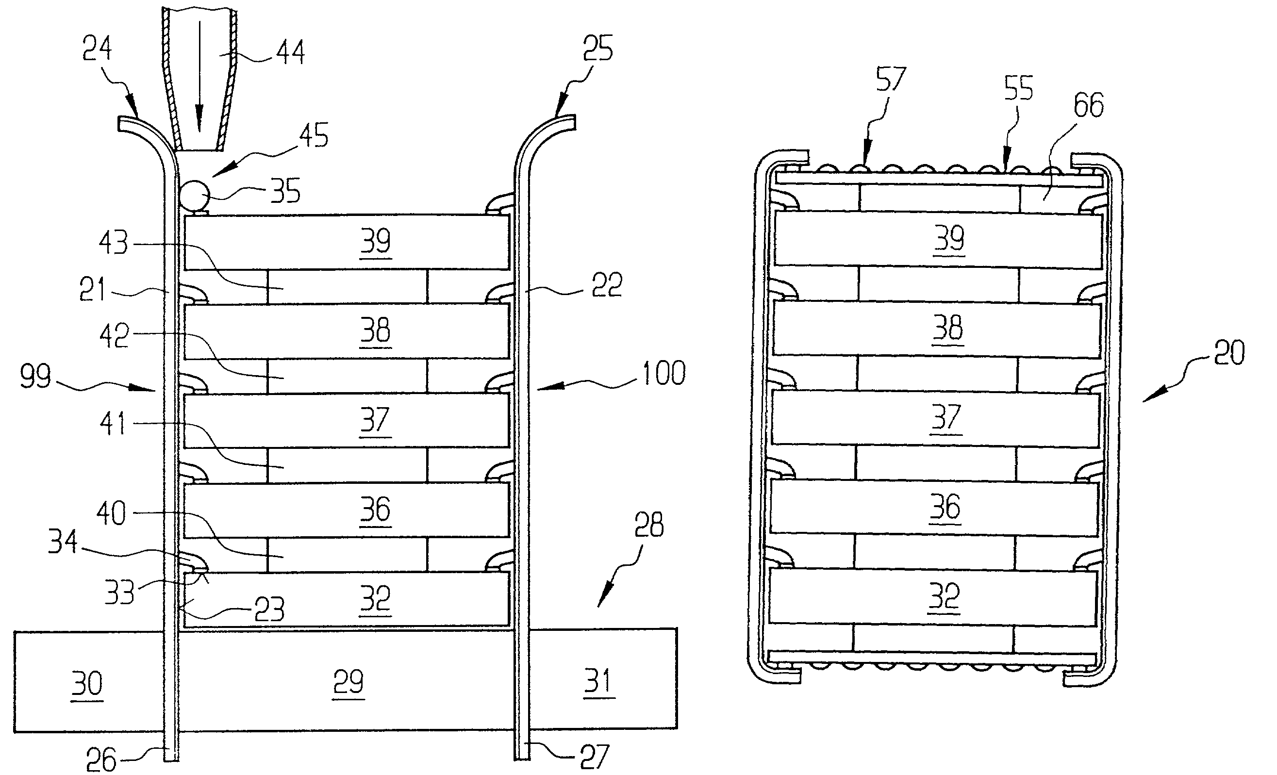
[0024]FIG. 1 shows a process stage in the course of the manufacture of a chip-stack arrangement 20 that is represented in FIG. 3 in its final state. With a view to forming the chip-stack arrangement 20 (FIG. 3), in the case of the embodiment example currently represented two flexibly constructed carrier substrate 21, 22 are arranged with their conducting-path structures 24, 25, comprising a plurality of conducting paths 23, located opposite one another. With a view to fixing the carrier substrates 21, 22 in the relative position represented in FIG. 1, the ends 26, 27 of the carrier substrates 21, 22 are accommodated in a clamping device 28. The clamping device 28 comprises in the present case a spacer block 29, against which the ends 26, 27 of the carrier substrates 21 and 22 respectively are held clamped by clamping jaws 30, 31. The spacer block 29 is so dimensioned that a first chip 32 can be positioned in the manner represented in FIG. 1 between the carrier substrates 21, 22 with...


PUM


Abstract

Process for the formation of a spatial chip arrangement having several chips (32, 36, 37, 38, 39) arranged in several planes and electrically connected to one another, in which the chips are connected via their peripheral connection surfaces (33) to assigned conducting paths (23) of a conducting-path structure (24, 25) arranged on at least one carrier substrate (21, 22) by the chips being arranged transverse to the longitudinal extent of the carrier substrate.

Description

[0001]This is a division of application Ser. No. 08 / 847,961 filed Apr. 22, 1997 which is incorporated herein by reference in its entirety. Ser. No. 09 / 553,123 filed Apr. 19, 2000 now abandoned, is also a division of application Ser. No. 08 / 847,961, which is now U.S. Pat. No. 6,281,577.BACKGROUND OF THE INVENTION[0002]The present invention relates to a process for the formation of a spatial chip arrangement having several chips arranged in several planes and electrically connected to one another, in which the chips are connected via their peripheral connection surfaces to assigned conducting paths of a conducting-path structure which is arranged on at least one carrier substrate by the chips being arranged transverse to the longitudinal extent of the carrier substrate.[0003]With the increasing miniaturisation of electronic appliances such as portable telephone for example, also generally designated as “handy”, or portable computers, known by the expression “notebook”, the demands reg...

Claims


Application Information

Patent Timeline
IPC IPC(8): G01R31/26H01L21/50H01L21/66H01L21/44H01L21/48H01L25/18H01L25/065H01L25/07
CPCH01L25/0652H01L25/0657H01L2225/06517H01L2225/06551H01L2225/06555H01L2924/0002H01L2225/06575H01L2225/06579H01L2924/00H01L25/065
Inventor OPPERMANN, HANS-HERMANNZAKEL, ELKEAZDASHT, GHASSEMKASULKE, PAUL
Owner PAC TECH PACKAGING TECH
Why Eureka
Try Eureka