

Method to fill the gap between coupled wafers
a technology of coupled wafers and coupled plates, applied in the direction of semiconductor devices, semiconductor/solid-state device details, electrical devices, etc., can solve the problems of mechanical stresses in the unsupported portions of the wafer being thinned
- Summary
- Abstract
- Description
- Claims
- Application Information
AI Technical Summary
Benefits of technology
Problems solved by technology
Method used
Image

Examples
Embodiment Construction
[0019]Embodiments of the present invention are three dimensional integrated circuit devices having a gap fill and their methods of formation. In the following description numerous specific details have been set forth in order to provide a thorough understanding of the present invention. In other instances, well-known semiconductor fabrication processes and techniques have not been set forth in particular detail in order to avoid unnecessarily obscuring the present invention.
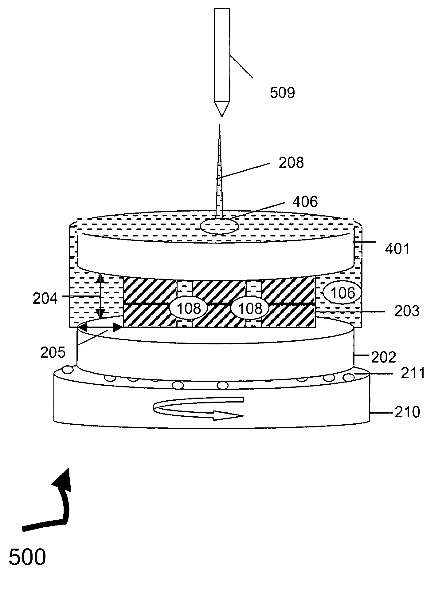
[0020]Embodiments of the present invention are a method for applying a material on a coupled wafer pair in order to fill a gap between wafers of the coupled wafer pair. Embodiments of the invention include applying a material through a hole within one of the wafers of the coupled wafer pair and creating a pressure differential to help the material flow between the coupled wafers. Embodiments of the invention include spinning a coupled wafer pair, applying a material on the top of or directly in a gap between the ...
PUM
 Abstract
Description
Claims
Application Information