Semiconductor light-emitting device and semiconductor light-emitting device

a technology of semiconductor light-emitting device and semiconductor light-emitting device, which is applied in the direction of semiconductor/solid-state device manufacturing, semiconductor devices, electrical devices, etc., can solve the problems of difficult to keep crystallinity at a high level, the inability to obtain good light-emitting characteristics, and the inability to form light-emitting elements in high precision

Inactive Publication Date: 2006-08-08
SAMSUNG ELECTRONICS CO LTD
View PDF5 Cites 451 Cited by
  • Summary
  • Abstract
  • Description
  • Claims
  • Application Information

AI Technical Summary

Benefits of technology

[0013]With the semiconductor light-emitting element of the present invention, the selective crystal growth layer is formed through selective growth, so that the selective crystal growth layer formed by the selective growth readily provides a required shape having different crystal planes on the surface thereof. Where the clad layer of the first conduction type, active layer and clad layer of the second conduction type are formed on the selectively crystal growth layer having different crystal planes on the surface thereof as extending in parallel to these crystal planes, the number of bonds may differ in every crystal plane. The difference in the number of bonds depending on the crystal plane will determine the amount of atoms being taken in, which influences a band gap energy. Thus, the amount of atoms being taken in, which influences the band gap energy, differs depending on the difference in crystal plane, with the result that regions having different light-emitting wavelengths can be obtained. The first light emission region and the second light emission region are, respectively, formed at such regions having different light-emitting wavelengths and are so arranged to be charged with an electric current thereinto, thereby enabling multi-color light emission from one element.
[0021]With the semiconductor light-emitting element of the present invention, the selective crystal growth layer is formed by selective growth, and the selective crystal grown layer formed by the selective growth may be readily formed as a required shape such as a hexagonal pyramid or a hexagonal trapezoid. Where the clad layer of a first conduction type, the active layer and the clad layer of a second conduction type are, respectively, formed on the selective crystal growth layer, these layers are influenced by the shape element of the selective crystal growth layer formed by the selective growth, resulting in different compositions and thicknesses depending on the underlying shape even if the layers of the same materials are used. Eventually, if the same types of active layers are used, different compositions appear or the thicknesses of such active layers differ from each other, thus leading to different band gap energies. Eventually, there are obtained regions whose light-emitting wavelengths differ from each other. In this way, the first light emission region and the second light emission region are, respectively, formed at regions having different light-emitting wavelengths, and are arranged so that an electric current is chargeable thereinto, thereby enabling the same element to permit multi-color light emission.

Problems solved by technology

However, with such a semiconductor light-emitting element having such a structure as set out above, the fabrication process becomes complicated, so that the light-emitting element cannot be formed in high precision.
Moreover, because crystallinity is degraded, good light-emitting characteristics cannot be obtained.
In general, however, a substrate and a semiconductor layer may suffer degradation in crystallinity depending on the manner of dry etching and, especially, where multiple etching cycles are performed, an element is formed through crystal growth from the surface of a substrate, where exposed by etching, in a second and subsequent etching cycles, thus making it difficult to keep crystallinity at a high level.
When multiple etching cycles are carried out, the numbers of the steps of mask alignment and etching increase correspondingly, resulting in the increased fabrication costs of the element.

Method used


Image

  • Semiconductor light-emitting device and semiconductor light-emitting device
  • Semiconductor light-emitting device and semiconductor light-emitting device
  • Semiconductor light-emitting device and semiconductor light-emitting device

Examples


example 1

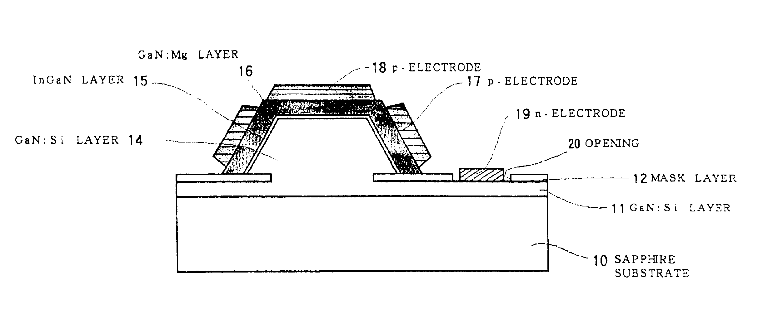
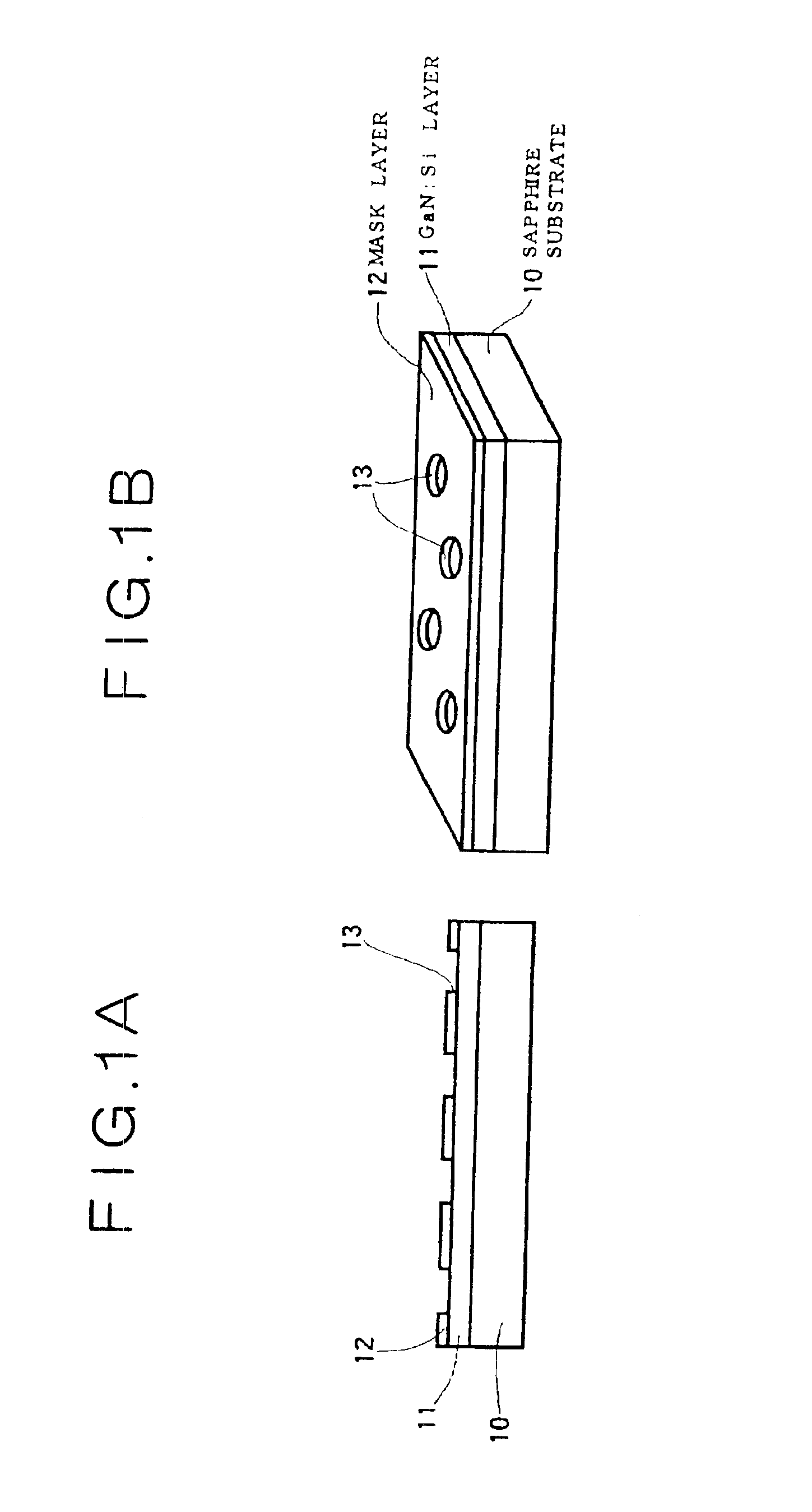
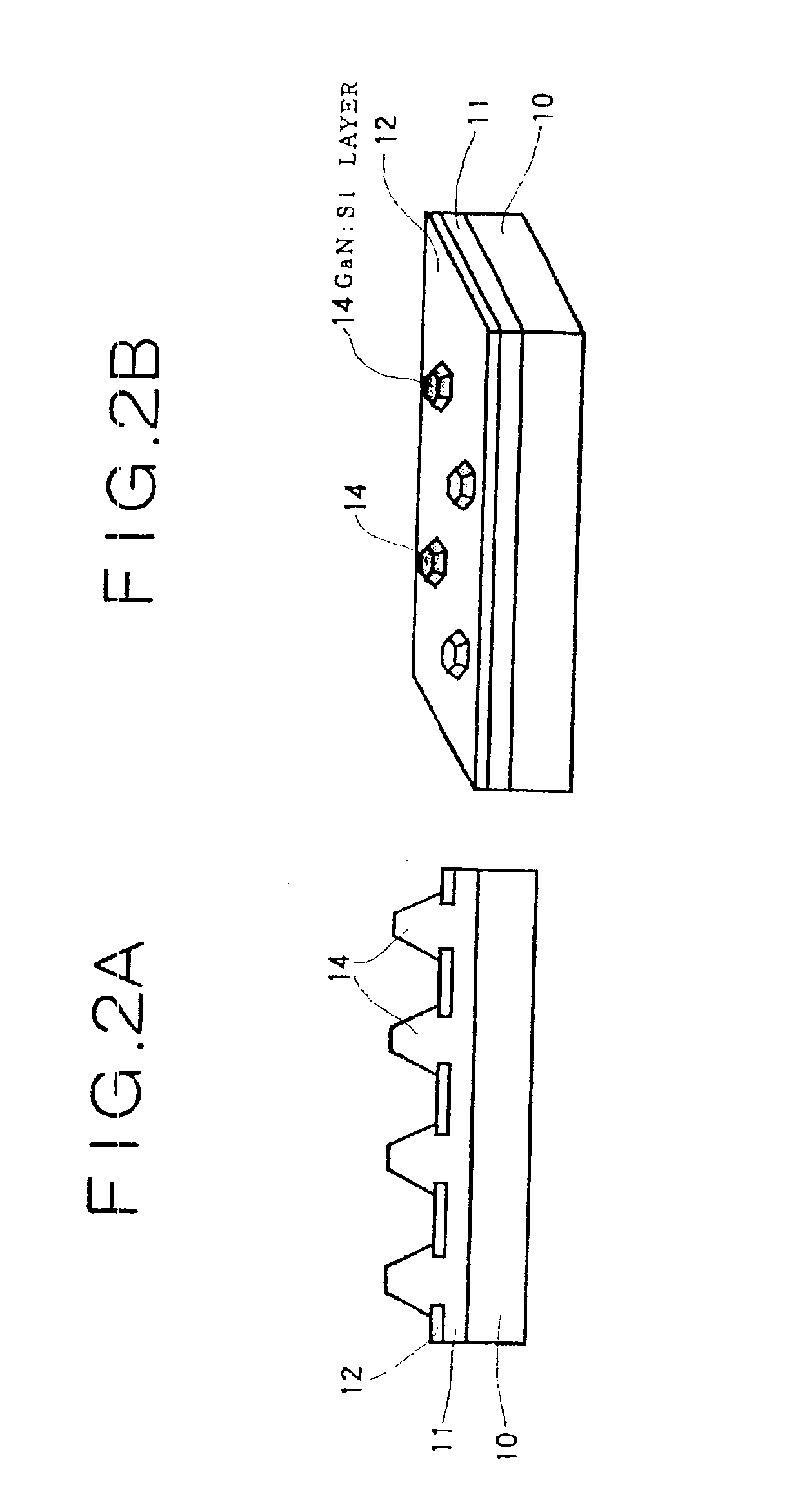
[0111]This example deals with direct selective growth on a sapphire substrate wherein a selective crystal growth layer having different crystal planes including an S plane and a C plane, and regions of the S plane and regions of the C plane are divided from each other and independent p-electrodes corresponding to two color light-emitting wavelengths are formed. With reference to FIGS. 1 to 6, an element structure is described along with a fabrication process thereof.

[0112]First, a low temperature buffer layer made of either AlN or GaN is formed on a sapphire substrate 10 having a C+ plane as a principal plane thereof at a low temperature of 500° C. Thereafter, a mask layer 12 made of SiO2 or SiN is formed over the entire surface in a thickness ranging from 100 to 500 nm, and openings 13 with a size of approximately 10 μm are formed according to photolithography by use of a hydrofluoric acid etchant (FIG. 1). In this example, the opening 13 is substantially in a round shape, and the ...

example 2

[0122]This example is one which deals with direct selective growth on a sapphire substrate wherein a selective crystal growth layer having an S plane is formed and independent p-electrodes corresponding to two color light-emitting wavelengths are formed on the plane portion and the side portion of the S plane. Referring to FIGS. 7 to 12, the element structure is described along with its fabrication process.

[0123]First, a low temperature buffer layer made of either AlN or GaN is formed on a sapphire substrate 30 having a C+ plane as a substrate principal plane at a low temperature of 500° C. After raising to a temperature of 1000° C., a silicon-doped GaN layer 31 is formed. Subsequently, a mask layer 32 made of SiO2 or SiN is formed over the entire surface in a thickness ranging from 100 to 500 nm, and openings 33 with a size of approximately 10 μm are formed according to photolithography using a hydrofluoric acid etchant (FIG. 7). In this example, the opening 33 is substantially in ...

example 3

[0133]This example is one which deals with direct selective growth on a sapphire substrate wherein a selective crystal growth layer having an S plane is formed and independent p-electrodes corresponding to three color light-emitting wavelengths are formed. Referring to FIGS. 13 to 18, the element structure is described along with its fabrication process.

[0134]First, a low temperature buffer layer made of either AlN or GaN is formed on a sapphire substrate 50 having a C+ plane as a substrate principal plane thereof at a low temperature of 500° C. After raising to a temperature of 1000° C., a silicon-doped GaN layer 51 is formed. Subsequently, a mask layer 52 made of SiO2 or SiN is formed over the entire surface in a thickness ranging from 100 to 500 nm, and openings 53 with a size of approximately 10 μm are formed according to photolithography using a hydrofluoric acid etchant (FIG. 13). In this example, the opening 53 is substantially in a round shape, and the size may be changed de...


PUM


Abstract

A semiconductor light-emitting element is provided which has a structure that does not complicate a fabrication process, can be formed in high precision and does not invite any degradation of crystallinity. A light-emitting element is formed, which includes a selective crystal growth layer formed by selectively growing a compound semiconductor of a Wurtzite type, a clad layer of a first conduction type, an active layer and a clad layer of a second conduction type, which are formed on the selective crystal growth layer wherein the active layer is formed so that the active layer extends in parallel to different crystal planes, the active layer is larger in size than a diffusion length of a constituent atom of a mixed crystal, or the active layer has a difference in at least one of a composition and a thickness thereof, thereby forming the active layer having a number of light-emitting wavelength regions whose emission wavelengths differ from one another. The element is so arranged that an electric current or currents are chargeable into the number of light-emitting wavelength regions. Because of the structure based on the selective growth, the band gap energy varies within the same active layer, thereby forming an element or device in high precision without complicating a fabrication process.

Description

BACKGROUND OF THE INVENTION[0001]The present invention relates to a semiconductor light-emitting element making use of a compound semiconductor having a Wurtzite-type crystal structure and also to a semiconductor light-emitting device, an image display device and an illumination device, each using such a semiconductor light-emitting element making use of the compound semiconductor as mentioned above. More particularly, the present invention relates to a semiconductor light-emitting element capable of emitting multi-color or white light by use of a compound semiconductor having a Wurtzite-type crystal structure and also to a semiconductor light-emitting device, an image display device and an illumination device.[0002]For a semiconductor light-emitting element, there is known an element which includes, entirely on a sapphire substrate, a builtup Iayer including a low temperature buffer layer, an n-type contact layer made of GaN doped with Si (silicon), an n-type clad layer made of Si-...

Claims


Application Information

Patent Timeline
Patent Type & Authority Patents(United States)
IPC IPC(8): H01L29/04H01L33/38H01L21/20H01L33/06H01L33/08H01L33/16H01L33/22H01L33/32
CPCH01L33/007H01L33/24H01L21/0237H01L21/0242H01L21/02639H01L21/0254H01L21/02576H01L21/02609H01L21/0262H01L21/02433H01L33/08H01L2224/48137
Inventor OKUYAMA, HIROYUKIDOI, MASATOBIWA, GOSHIOOHATA, TOYOHARU
Owner SAMSUNG ELECTRONICS CO LTD
Why Eureka
Try Eureka