Power supply circuit for vacuum fluorescent display

a technology of power supply circuit and vacuum fluorescent display, which is applied in the direction of tubes with screens, process and machine control, instruments, etc., can solve the problems of high noise, high cost and time, and light emission leakage, and achieve the effect of low nois

Active Publication Date: 2006-08-08
NORITAKE CO LTD +1
View PDF3 Cites 7 Cited by
  • Summary
  • Abstract
  • Description
  • Claims
  • Application Information

AI Technical Summary

Benefits of technology

[0013]It is an object of the present invention to eliminate the necessity of a filament-driving transformer and achieve low noise.
[0014]It is another object of the present invention to shorten the time required for the design of a power supply.
[0015]It is still another object of the present invention to prevent flicker when a desired pattern is displayed on a vacuum fluorescent display tube.
[0016]It is still another object of the present invention to achieve low power consumption.

Problems solved by technology

In a vacuum fluorescent display, when the filament potential drops below the turn-off level of the anode potential, light emission leakage may occur.
In the above conventional power supply circuit 400, however, since the AC filament voltage Ef is obtained by using the transformer 9, problems (1) to (4) are posed as follows:(1) producing much noise;(2) requiring much cost and time for the design of a power supply;(3) causing flicker when displaying a desired pattern on the vacuum fluorescent display tube 1; and(4) requiring a large power consumption.

Method used


Image

  • Power supply circuit for vacuum fluorescent display
  • Power supply circuit for vacuum fluorescent display
  • Power supply circuit for vacuum fluorescent display

Examples


first embodiment

[First Embodiment]

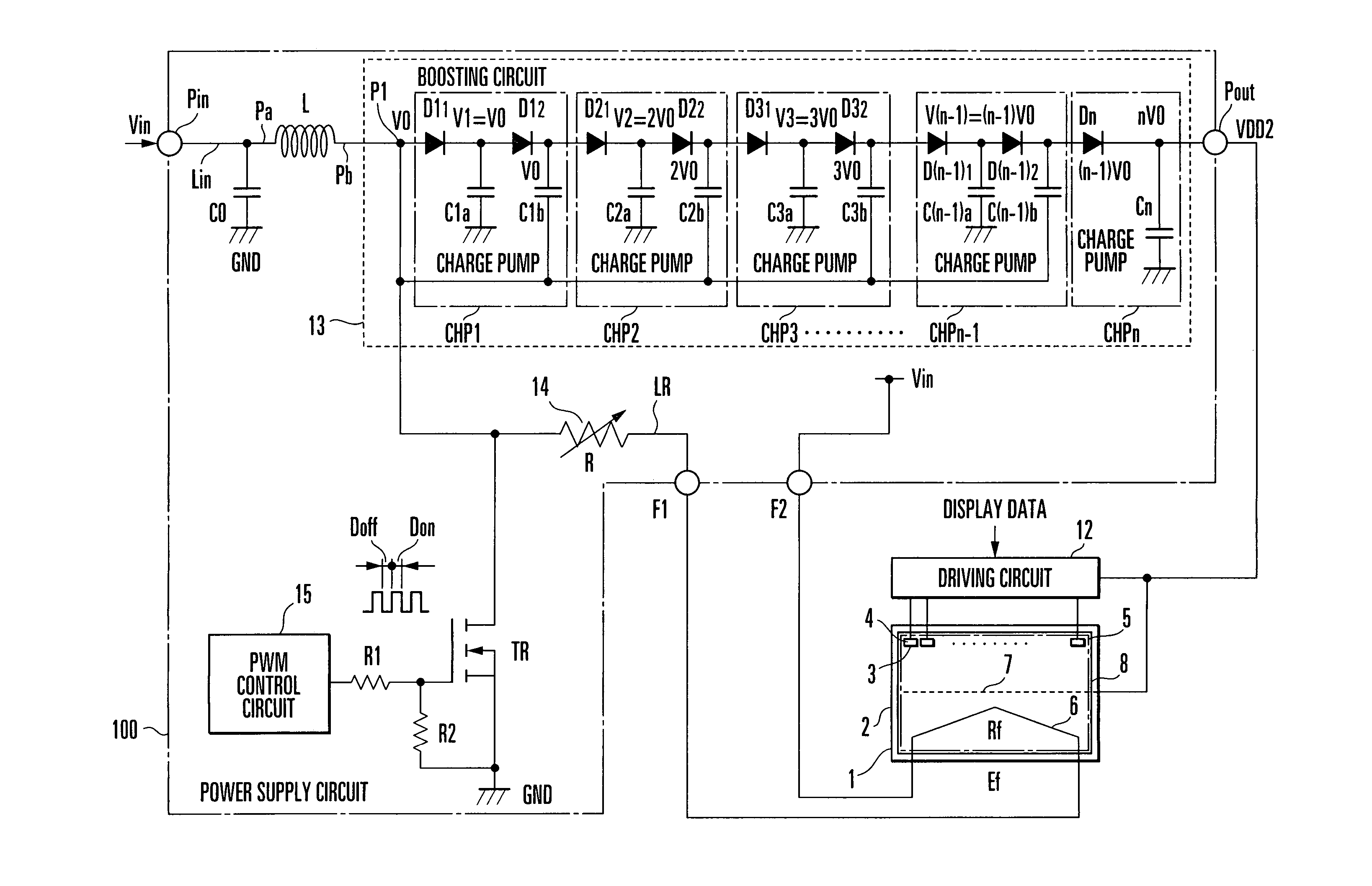
[0036]FIG. 1 shows the main part of a power supply circuit according to an embodiment (first embodiment) of the present invention. A power supply circuit 100 includes a capacitor (input smoothing capacitor) C0, a boosting coil (induction element) L, a boosting circuit 13, a switching transistor (field-effect transistor) TR, a variable resistor (voltage adjustment resistor) 14, a PWM control circuit 15, and resistors R1 and R2. The power supply circuit has an input terminal Pin, output terminal Pout, filament terminal F1 (first terminal), and a filament terminal F2 (second terminal).

[0037]An input voltage (DC voltage) Vin is applied to the input terminal Pin. A DC voltage VDD2 for the anode / grid is output from the output terminal Pout. A cathode (filament) 6 of a vacuum fluorescent display tube 1 is connected between the filament terminals F1 and F2.

[0038]In the power supply circuit 100, the boosting coil L is provided in a current path Lin between the input termina...

second embodiment

[Second Embodiment]

[0067]FIG. 4 shows the main part of a power supply circuit according to another embodiment (second embodiment) of the present invention. A power supply circuit 200 includes a control circuit 16A, boosting circuit 17, and cutoff circuit 18A, and has an input terminal Pin, output terminal Pout, and filament terminals F1 and F2. A DC voltage (input voltage) Vin is applied to the input terminal Pin. A DC voltage VDD2 for the anode / grid is output from the output terminal Pout. A cathode (filament) 6 of a vacuum fluorescent display tube 1 is connected between the filament terminals F1 and F2.

[0068]The cutoff circuit 18A includes a first switch SW1, second switch SW2, resistor R, diodes D1 and D2, and capacitors C1 and C2. The switches SW1 and SW2 are connected in series between an input line Lin for a DC voltage Vin and a ground line (GND). In this series connection, the switch SW1 is located on the input line Lin side of the DC voltage Vin and the switch SW2 is located...

third embodiment

[Third Embodiment]

[0098]FIG. 8 shows an application of the power supply circuit 200 shown in FIG. 4. In a power supply circuit 300, third and fourth switches SW3 and SW4 are connected in series between an input line Lin for a DC voltage Vin and a ground line. In this series connection circuit, the switch SW3 is located on the input line Lin side of the DC voltage Vin, and the switch SW4 is located on the ground line side. A capacitor C2 is connected between a filament terminal F2 and a node PB between the switches SW3 and SW4.

[0099]A switch SW1 and the switch SW4 constitute a first switch pair, and a switch SW2 and the switch SW3 constitute a second switch pair. A control circuit 16B periodically and alternately turns on / off the first switch pair (SW1 and SW4) and the second switch pair (SW2 and SW3) in opposite directions.

[0100]That is, the control circuit 16B periodically repeats the operation of “simultaneously turning off the second switch pair (SW2 and SW3) when simultaneously ...


PUM


Abstract

A power supply circuit for a vacuum fluorescent display includes a boosting coil, input terminal, switching transistor, PWM control circuit, boosting circuit, first filament terminal, and second filament terminal. The boosting coil is provided in a current path to generate an induced voltage in accordance with a change in current flowing therein. The input terminal receives a DC voltage to be applied to one terminal of the boosting coil. The switching transistor is provided between the other terminal of the boosting coil and a ground line. The PWM control circuit periodically turns on / off the switching transistor. The boosting circuit generates a boosted voltage on the basis of an induced voltage generated at the other terminal of the boosting coil when the switching transistor is switched from ON to OFF. The first terminal is connected to the node between the other terminal of the boosting coil and the switching transistor. A DC voltage lower than the induced voltage generated at the other terminal of the boosting coil is applied to the second terminal.

Description

BACKGROUND OF THE INVENTION[0001]The present invention relates to a power supply circuit attached to a vacuum fluorescent display.[0002]A vacuum fluorescent display is an electron tube which displays a desired pattern by causing electrons emitted from the cathode in the vacuum vessel (envelope) having at least one side which is transparent to impinge on the phosphor applied to the anode and causing the phosphor to emit light. In general, as this vacuum fluorescent display, a display having a triode structure with a grid for controlling the behavior of electrons is most frequently used.[0003]FIG. 15 shows a conventional general vacuum fluorescent display tube and a circuit attached to the vacuum fluorescent display (see Japanese Patent Laid-Open No. 2002-260565 (reference 1)). Referring to FIG. 15, reference numeral 1 denotes a vacuum fluorescent display tube; and 400, a power supply circuit attached to the vacuum fluorescent display tube 1. In the vacuum fluorescent display tube 1, ...

Claims


Application Information

Patent Timeline
Patent Type & Authority Patents(United States)
IPC IPC(8): G05F1/10G05F1/40G09G3/20H01J31/15G09G3/22
CPCG09G3/22G09G2330/02H01J31/15
Inventor KAMEDA, MASASHISHIBATA, KAZUHISANAKANISHI, HIROSHITERAKAMI, SHINICHIEGUCHI, TOSHIHIDE
Owner NORITAKE CO LTD
Why Eureka
Try Eureka