Planarizing sacrificial oxide to improve gate critical dimension in semiconductor devices

a semiconductor device and critical dimension technology, applied in the field of planarizing sacrificial oxide to improve the critical dimension of the gate in the semiconductor device, can solve the problems of increasing difficulty in overcoming, short channel effect, and the reduction of design features below 100 nm, and achieve the effect of improving the critical dimension of the ga

Inactive Publication Date: 2006-08-15
ADVANCED MICRO DEVICES INC
View PDF14 Cites 10 Cited by
  • Summary
  • Abstract
  • Description
  • Claims
  • Application Information

AI Technical Summary

Benefits of technology

[0005]Implementations consistent with the present invention provide a method of forming a FinFET device that improves a critical dimension (CD) of the gate. A sacrificial layer formed over the gate material may be planarized before gate patterning. In addition, an antireflective coating may be formed on the planarized sacrificial layer.

Problems solved by technology

The reduction of design features below 100 nm challenges the limitations of conventional methodology.
For example, when the gate length of conventional planar metal oxide semiconductor field effect transistors (MOSFETs) is scaled below 100 nm, problems associated with short channel effects, such as excessive leakage between the source and drain, become increasingly difficult to overcome.
In addition, mobility degradation and a number of process issues also make it difficult to scale conventional MOSFETs to include increasingly smaller device features.

Method used


Image

  • Planarizing sacrificial oxide to improve gate critical dimension in semiconductor devices
  • Planarizing sacrificial oxide to improve gate critical dimension in semiconductor devices
  • Planarizing sacrificial oxide to improve gate critical dimension in semiconductor devices

Examples


Embodiment Construction

[0021]The following detailed description of the invention refers to the accompanying drawings. The same reference numbers in different drawings may identify the same or similar elements. Also, the following detailed description does not limit the invention. Instead, the scope of the invention is defined by the appended claims and their equivalents.

[0022]Implementations consistent with the present invention provide a method of forming a FinFET device that improves a smallest feature size in the gate. To improve the smallest feature size, the gate material may be planarized before gate patterning. In addition, an antireflective coating may be formed on the planarized gate material.

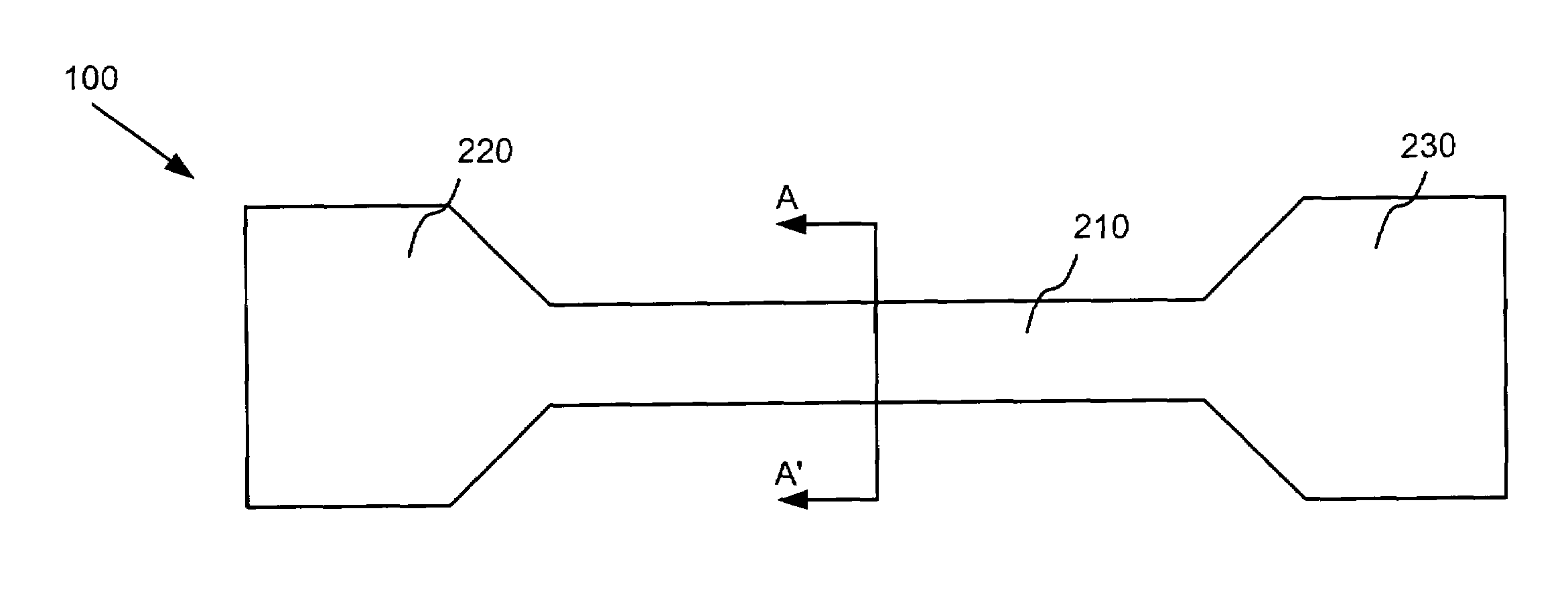
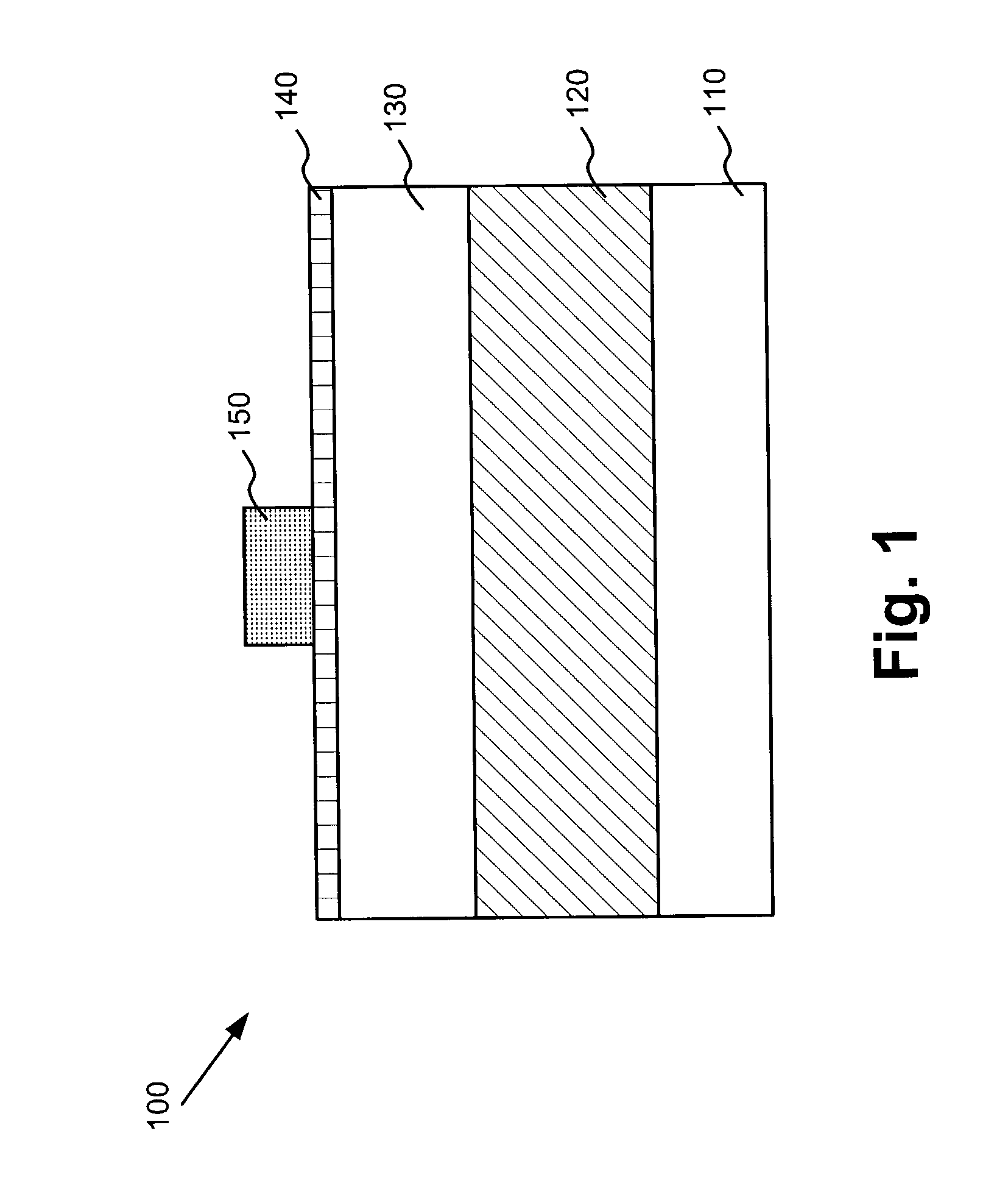
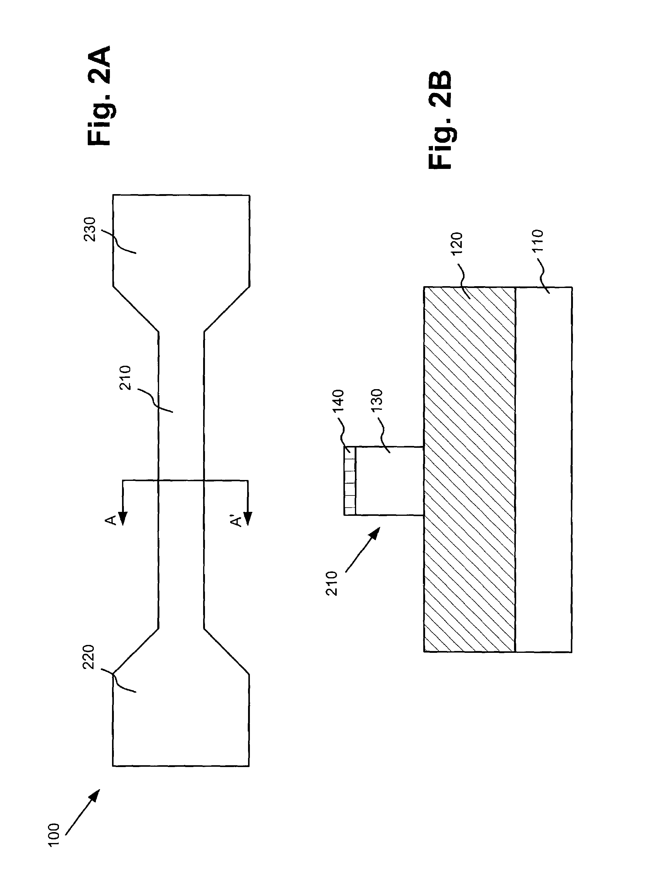
[0023]FIG. 1 illustrates the cross-section of a semiconductor device 100 formed in accordance with an exemplary embodiment of the present invention. Referring to FIG. 1, semiconductor device 100 may include a silicon on insulator (SOI) structure that includes a silicon substrate 110, a buried oxide layer 120...


PUM


Abstract

A method of manufacturing a semiconductor device may include forming a fin structure on an insulator and depositing a gate material over the fin structure. The method may also include forming a sacrificial material over the gate material and planarizing the sacrificial material. An antireflective coating may be deposited on the planarized sacrificial material. A gate structure may then be formed by etching the gate material.

Description

TECHNICAL FIELD[0001]The present invention relates to semiconductor devices and methods of manufacturing semiconductor devices. The present invention has particular applicability to double-gate devices.BACKGROUND ART[0002]The escalating demands for high density and performance associated with ultra large scale integration semiconductor devices require design features, such as gate lengths, below 100 nanometers (nm), high reliability and increased manufacturing throughput. The reduction of design features below 100 nm challenges the limitations of conventional methodology.[0003]For example, when the gate length of conventional planar metal oxide semiconductor field effect transistors (MOSFETs) is scaled below 100 nm, problems associated with short channel effects, such as excessive leakage between the source and drain, become increasingly difficult to overcome. In addition, mobility degradation and a number of process issues also make it difficult to scale conventional MOSFETs to inc...

Claims


Application Information

Patent Timeline
Patent Type & Authority Patents(United States)
IPC IPC(8): H01L21/00
CPCH01L29/785H01L29/66795
Inventor AHMED, SHIBLY S.TABERY, CYRUS E.YU, BIN
Owner ADVANCED MICRO DEVICES INC
Why Eureka
Try Eureka