Method and means for reducing electromagnetic noise induced in X-ray detectors

a technology of electromagnetic noise and detectors, applied in the field of reducing electromagnetic noise in x-ray detectors, can solve the problems of complex solid-state systems that are inherently more susceptible to electric and/or magnetic (referred to as electro-magnetic noise) noise, and the design of a/d conversion systems has become increasingly complex

Active Publication Date: 2006-08-15
GENERAL ELECTRIC CO
View PDF6 Cites 18 Cited by
  • Summary
  • Abstract
  • Description
  • Claims
  • Application Information

AI Technical Summary

Benefits of technology

[0008]One embodiment relates to method for reducing electromagnetic noise induced in an X-ray detector. This embodiment comprises locally sampling an interfering field in the X-ray detector and subtracting an amplitude / magnitude of the sampled interfering field from at least one element sample. The method further comprises outputting at least one sample having reduced EM noise.
[0014]Still another embodiment relates to an X-ray detector used in a medical imaging system. In this embodiment, the X-ray detector comprises a panel portion, at least one edge finger contact and a readout electronics portion. The at least one field sensing conductor is adapted to reduce electromagnetic noise induced in the X-ray detector. The at least one edge finger contact is coupled to at least a portion of the panel portion and the readout electronics portion.

Problems solved by technology

At the same time, in order to handle the smaller and lengthier data line paths and still produce acceptable image quality, the design of the A / D conversion system has become increasingly complex.
However, such complex solid state systems have become inherently more susceptible to electric and / or magnetic (referred to as Electro-Magnetic or “EM”) noise induced onto the photo sensor panel (induced primarily onto the data line paths).
Effective shielding of low and high frequency, Electro-Magnetic noise is not possible using current materials, as low frequency magnetic fields require metallic elements which greatly attenuate X-ray photons in medical applications.

Method used


Image

  • Method and means for reducing electromagnetic noise induced in X-ray detectors
  • Method and means for reducing electromagnetic noise induced in X-ray detectors
  • Method and means for reducing electromagnetic noise induced in X-ray detectors

Examples


Embodiment Construction

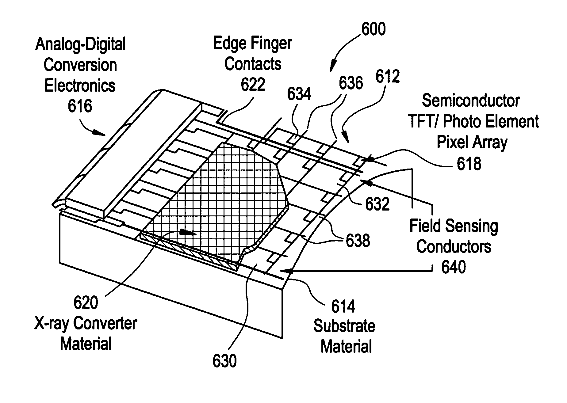
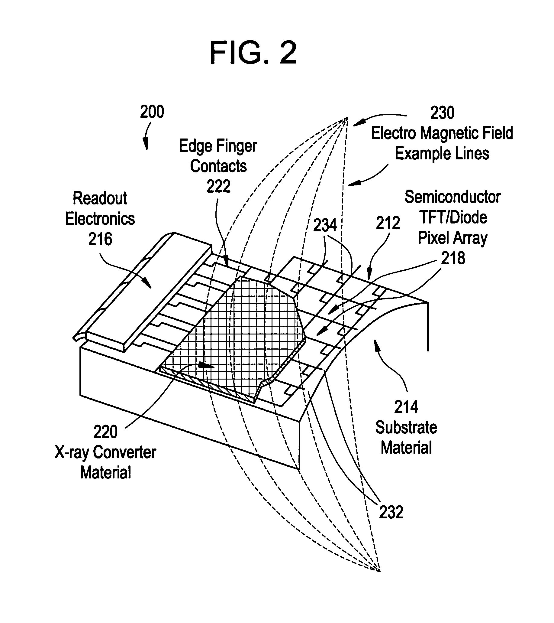
[0029]For the purpose of illustration only, the following detailed description references certain embodiments of an X-ray detector (a flat panel X-ray detector) used in a medical imaging system, device, machine or apparatus. However, it is understood that the present invention may be used with other devices or systems.

[0030]It should be appreciated that the engineering and manufacture of active or flat panels, used in X-ray detectors for example, is a complex endeavor. Such engineering and manufacturing process requires knowledge of amorphous or single / poly crystaline semiconductor devices such as Thin Film Transistors Field Effect Transistors (TFT FET) and wide bandgap Photodiodes for example. Deposition processes such as Plasma Enhanced Chemical Vapor Deposition (alternatively referred to as “PECVD”) and sputtering for example are used to produce interconnecting metal, device structures, X-ray converters and other structures in such engineering and manufacturing processes.

[0031]It...


PUM


Abstract

The present invention relates to a system and method by which the magnitude of an interfering electrical and / or magnetic field may be sampled locally (in the X-ray detector for example) and reduced or eliminated. More specifically, embodiments comprise a system and method by which an interfering field may be sampled within the same orientation as the X-ray detector panel, and then subtracted out of each respective element sample.

Description

BACKGROUND OF THE INVENTION[0001]This application is directed in general to the design and manufacture of an X-ray detector and an X-ray detector formed thereby. Specifically, this application is directed to the design and manufacture of flat panel X-ray detectors and the flat panel X-ray detectors formed thereby, which in turn may be used in medical imaging systems, devices or other apparatus for example.[0002]It should be appreciated that engineering and manufacturing flat panels adapted to be used in X-ray detectors for example, is a complex endeavor. Solid state X-ray imaging technology has steadily advanced due in part to the development of photo sensitive semiconductor arrays using either indirect X-ray-to-light scintillation panels (Amorphous Silicon with CsI for example) or direct X-ray conversion panels (Amorphous SE, PbO or Hgl for example). It is contemplated that one or more of those technologies may use transistor switches (TFT-FETs for example) providing effective mult...

Claims


Application Information

Patent Timeline
Patent Type & Authority Patents(United States)
IPC IPC(8): G01T1/24H01L27/00H01L27/146G21K7/00G01T1/20A61B6/00A61B6/12G06T11/00H01L27/14H01L31/09H04N5/32H04N5/357H05G1/26
CPCA61B6/00A61B6/12A61B6/4233H04N5/32H04N3/155H04N5/217A61B6/547H04N25/617H04N23/81
Inventor KAUTZER, JEFFREY A.CRONCE, RICHARD GORDONKUKRER, OLGUN
Owner GENERAL ELECTRIC CO
Why Eureka
Try Eureka