Semiconductor device

a technology of semiconductors and devices, applied in the direction of logic circuit coupling/interface arrangements, pulse techniques, instruments, etc., can solve the problems of large load due to pixels, inability of the inverter itself to supply a sufficient amount of electric, and extreme complexity of the process, so as to reduce the number of buffers and the like, the effect of increasing the load driving capability

Inactive Publication Date: 2006-08-15
SEMICON ENERGY LAB CO LTD
View PDF60 Cites 69 Cited by
  • Summary
  • Abstract
  • Description
  • Claims
  • Application Information

AI Technical Summary

Benefits of technology

[0032]As shown in FIG. 1A, there is a structure in which two TFTs are added to the structure of FIG. 13A. The TFTs 1302 and 1303 in FIG. 13A have roles for boot strap operation and for electrical charge and discharge of a load of a latter stage. However, TFTs 102 and 103 contribute only to boot strap operations in the structure shown in FIG. 1A, and TFTs 105 and 106 are formed as TFTs that perform electrical charge and discharge of a load. With such structure, it is possible to obtain good operation with no loss of function even in the case in which the load attached to a later stage becomes somewhat large.
[0038]The load driving capability can be increased with such structure, and therefore the number of stages for buffers and the like can be made smaller, which lead to redaction in the surface area occupied by circuits.

Problems solved by technology

This is because the CMOS itself inverter does not have the capability of supplying a sufficient amount of electric charge for driving the load.
The load due to the pixels is therefore large.
The extreme complexity of the processes therefore invites an increase in manufacturing costs.
In addition, in the case in which the driver circuit and the pixel portion are formed integrally on the substrate as discussed above, some defects become a problem which affects the entire manufactured product, and has a large influence on yield.
This is because, although there are many cases in which the voltage between the gate and the source is considered in explaining TFT operation, it is difficult to clearly differentiate the source region and the drain region of the TFT based upon the structure of the TFT and the use of unified names may, instead of being helpful, lead to confusion developing.
Similarly, attenuation of the amplitude due to the threshold voltage continues to develop and overlap throughout the stages, the amplitude of the waveform shrinks rapidly, and the circuit cannot function as a satisfactory circuit.

Method used


Image

  • Semiconductor device
  • Semiconductor device
  • Semiconductor device

Examples


embodiment 1

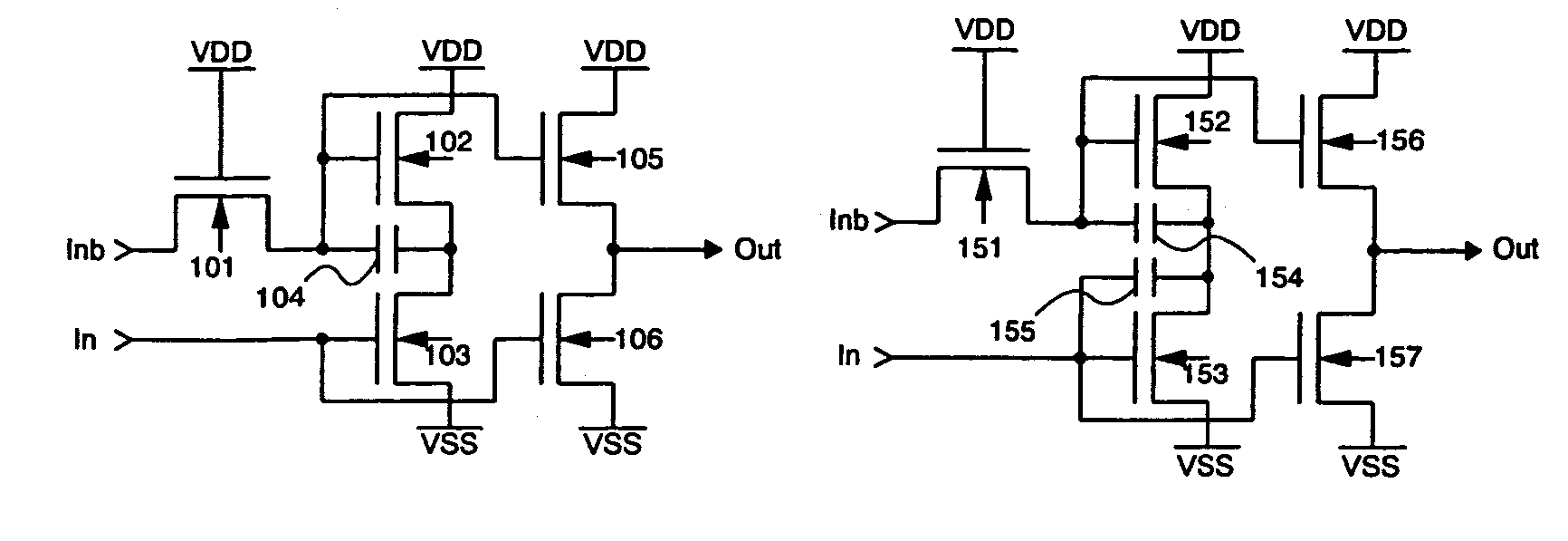
[0154]In the circuits shown in FIGS. 1A and 1B and explained in the Embodiment Mode, the role of placing the gate electrode of the TFT 102 in a floating state is accomplished by only the TFT 101. There is the fact discussed above that the gate electrode of the TFT 102 is placed in a floating state when the electric potential of the gate electrode of the TFT 102 becomes (VDD−VthN). If the H level of the input signal is not satisfy (VDD−VthN), the TFT 101 does not turn off, and therefore the gate electrode of the TFT 102 is not placed in a floating state, and accordingly the boot strap does not work.

[0155]The circuit shown in FIG. 9A is used in the above case. A difference between the circuits shown in FIG. 9A and in FIG. 1A is that two TFTs, a TFT 901 and a TFT 902, are used in order to place a gate electrode of a TFT 903 in a floating state. The above stated condition is considered with the circuit of FIG. 9A. The voltage amplitude of an input signal is VDD0(Hi) to VSS(Lo), and the ...

embodiment 2

[0160]This embodiment gives a description on a method of manufacturing TFTs for driving circuit provided in a pixel portion and in the periphery of the pixel potion formed on the same substrate. Note that the processes of manufacturing of a liquid crystal device is described as an example here, as mentioned above, there is no particular limitation on the liquid crystal display device.

[0161]First, as shown in FIG. 7A, a base film 5002 is formed from an insulating film such as a silicon oxide film, a silicon nitride film, and a silicon oxynitride film on a glass substrate 5001. The substrate 5001 is formed of barium borosilicate glass typical example of which is Corning #7059 glass or Corning #1737 glass (product of Corning Incorporated), or of aluminoborosilicate glass. The base film 5002 is, for example, (not shown) a laminate of a silicon oxynitride film that is formed from SiH4, NH3, and N2O by plasma CVD to a thickness of 10 to 200 nm (preferably 50 to 100 nm) and a silicon oxyni...

embodiment 3

[0192]An example of manufacturing a display device which has the circuit as shown in the Embodiment Mode and Embodiment 1 is discussed in Embodiment 3.

[0193]A schematic diagram of the display device is shown in FIG. 10A. A pixel portion 1001 is placed in a center portion of a substrate 1000. A source signal line driver circuit 1002 for controlling source signal lines, and gate signal line driver circuits 1007 for controlling gate signal lines are formed in the periphery of the pixel portion 1001. Although the gate signal line driver circuits 1007 are placed symmetrically on both side of the pixel portion 1001, there may be a gate signal driver circuit formed on only one side thereof.

[0194]Signals input from the outside for driving the source signal line driver circuit 1002 and the gate signal line driver circuits 1007 are input through an FPC 1010. The signals input from the FPC 1010 have small voltage amplitudes, and therefore undergo transformation of the voltage amplitudes by lev...


PUM


Abstract

A circuit with a large load driving capability, which is structured by single polarity TFTs, is provided. With a capacitor (154) formed between a gate electrode and an output electrode of a TFT (152), the electric potential of the gate electrode of the TFT (152) is increased by a boot strap and normal output with respect to an input signal is obtained without amplitude attenuation of an output signal due to the TFT threshold value. In addition, a capacitor (155) formed between a gate electrode and an output electrode of a TFT (153) compensates for increasing the electric potential of the gate electrode of the TFT (152), and a larger load driving capability is obtained.

Description

CROSS-REFERENCE TO RELATED APPLICATIONS[0001]This application is a continuation application of U.S. application Ser. No. 10 / 202,861, filed Jul. 26, 2002 now a U.S. Pat. No. 6,788,108 which claims the benefit of a foreign priority application filed in Japan as Ser. No. 2001-229054 on Jul. 30, 2001. This application claims priority to each of these prior applications, and the disclosures of the prior applications are considered part of (and are incorporated by reference in) the disclosure of this application.BACKGROUND OF THE INVENTION[0002]1. Field of the Invention[0003]The present invention relates to an inverter, buffer, and level shifter, and to a semiconductor device using them. Note that the term display device used within this specification includes a liquid crystal display device which employ liquid crystal elements in pixels, and a light emitting device which employ light emitting elements such as electro-luminescence (EL) elements. The term semiconductor device indicates cir...

Claims


Application Information

Patent Timeline
Patent Type & Authority Patents(United States)
IPC IPC(8): H03K19/0175H01L51/50G09G3/20G09G3/30G09G3/32G09G3/36G11C19/00G11C19/28H01L21/77H01L21/84H01L27/12H01L27/32H01L29/786H03K19/017H05B33/14
CPCG09G3/20H01L27/1214H01L29/78621H03K19/01714H01L2029/7863G09G3/3275G09G3/3648G09G2300/08G09G2310/0218G09G2310/0267G09G2310/027G09G2310/0275G09G2310/0286G09G2310/0289H01L27/3244H01L51/5206H01L51/5221H01L2251/5315G09G3/3208H01L27/1255H10K59/123H10K2102/3026H10K59/80518H10K59/8052H10K50/82H10K50/818
Inventor MIYAKE, HIROYUKISHIONOIRI, YUTAKA
Owner SEMICON ENERGY LAB CO LTD
Why Eureka
Try Eureka