Optical cross connect

a cross-connecting and optical technology, applied in the field of optical cross-connecting, can solve the problems of compromising the efficiency of the overall system, high energy input signal, large and expensive optical cross-connecting, etc., and achieves the effects of reducing the number of nodes

Inactive Publication Date: 2006-08-15
TYCO ELECTRONICS NETHERLAND BV
View PDF2 Cites 42 Cited by
  • Summary
  • Abstract
  • Description
  • Claims
  • Application Information

AI Technical Summary

Benefits of technology

[0014]The present invention provides for a high-density, high-capacity modular optical cross-connect that is scalable to a user's particular application. Applicants recognize that by forming the cross-connect from similar modules, it can be sized to a particular need using modular components in the form of stackable trays and optical circuits contained within the trays. The optical circuits themselves can be relatively few in design and based upon reliable technology. Additionally, applicants recognize that by configuring the input nodes perpendicular to the output nodes, the optical cross-connect can be defined in three dimensions instead of two thereby increasing node density.
[0015]In a preferred embodiment, the optical cross-connect comprises comprising a three-dimensional array of fibers in which one end of each fiber is presented on a first face, and the other end of each fiber is presented on a second face such that the first and second faces present rows and columns of groupings of fibers and wherein the input nodes are defined along the rows of the first face and the output nodes are defined along the columns of the second face. Preferably, the rows are contained within removable trays to impart versatility to the system.

Problems solved by technology

First, the fact that optical signals are converted to electrical signals and then back to optical signals necessarily requires components for affecting the electrical / optical conversion.
These additional components tend to make the optical cross connect large and expensive.
Additionally, the additional components compromise the efficiency of the overall system thereby requiring higher energy input signals and increased reliance on optical amplifiers to raise the input signals to the appropriate level.
Finally, by converting between the optical and electrical domains and switching in the electrical domain, optoelectric cross-connects are slower and encounter electrical historesis which limits the speed of switching.
Therefore, although used traditionally, the optoelectric approach to cross connects is faced with inherent problems.
Although the optical cross-connect as described above offers significant advantages over optoelectric devices and overcomes many of their shortcomings, trends in the industry somewhat militate against its general acceptance.
Furthermore, despite these trends, there is no “standard” industry cross-connect.
The applicants have identified a number of issues which somewhat restrict the ability of the optical circuit described above to meet current industry trends.
Applicants recognize that as the number of nodes increases from 8 up through 64 and beyond, the area required to accommodate the flat fiber circuit and the complexity of the fiber layouts thereon become prohibitive.
Additionally, designing and manufacturing specific optical circuits to meet particular application needs is impractical.
Specifically, designing an optical circuit layout requires attention to a variety of factors including minimum bend radius, skew, plus other problems, such as minimizing fiber stacking and securing fibers to a substrate.
It is impractical that specific optical circuits be designed and manufactured according to specific applications.

Method used


Image

  • Optical cross connect
  • Optical cross connect
  • Optical cross connect

Examples


Embodiment Construction

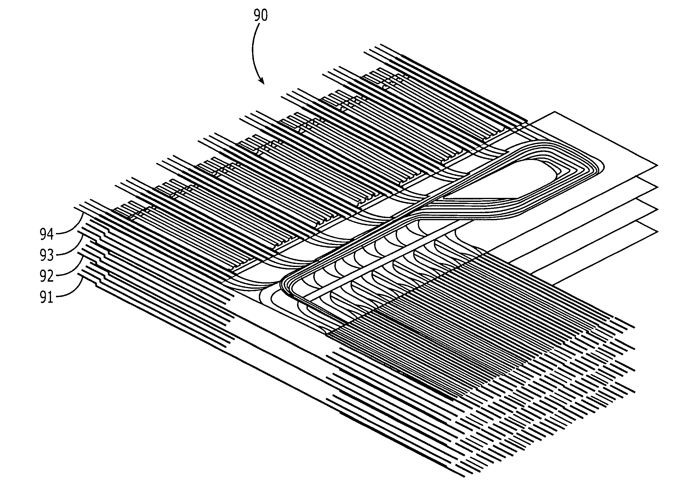
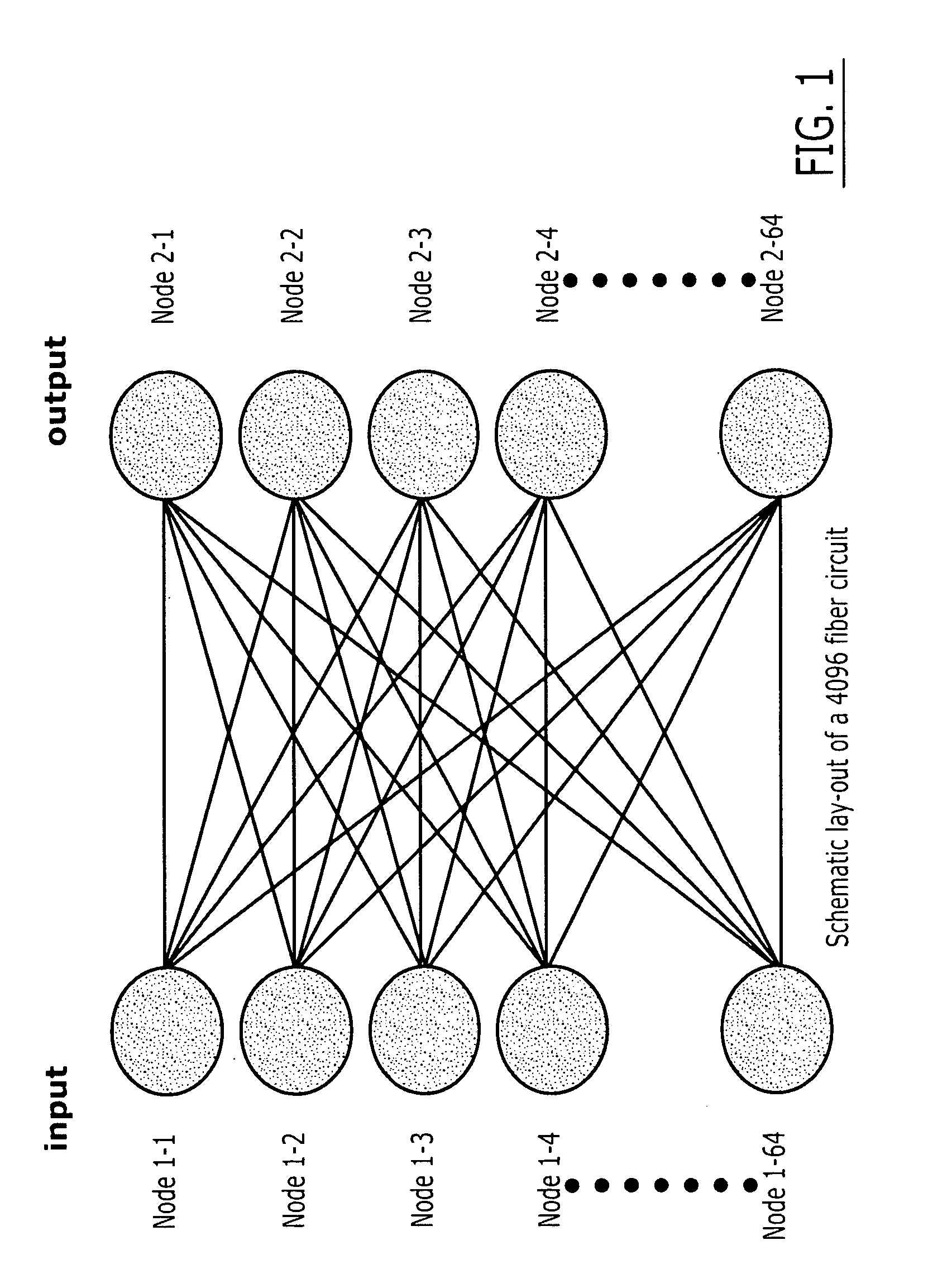
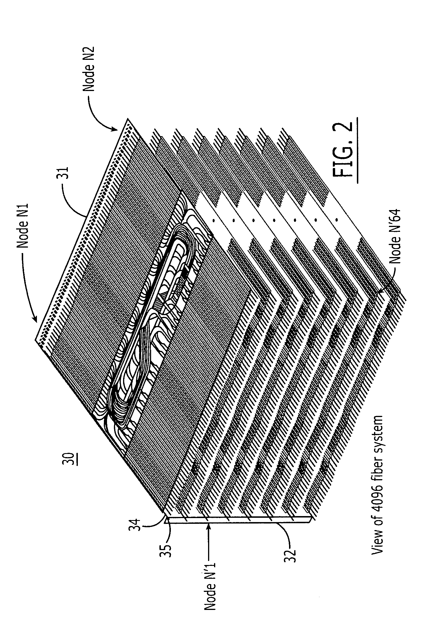
[0024]Referring to FIGS. 3 through 9, a preferred embodiment of the optical cross connect of the present invention and its components are shown. FIG. 3 shows a preferred embodiment of a 64×64 node, 4,096 fiber perfect shuffle. Although the depicted system comprises 64×64 nodes, it should be understood that the present invention is not limited to a particular cross-connect configuration. Indeed, the configurability of the optical cross-connect is an important feature of the invention. The optical cross-connect can be figured to meet any desired node interconnection, for example, 8×8, 16×16, 32×32 and as shown 64×64, as discussed below.

[0025]As shown in FIG. 3, the optical cross-connect system 30 comprises a three-dimensional array of interconnected fibers 31. The fibers are arranged so that their ends are presented essentially on two different faces, 32, 33, of the three-dimensional array. It should be understood that the term “face,” as used herein, is not intended to imply that all...


PUM


Abstract

An optical cross-connect system (30) for interconnecting optical pathways of a horizontal node with each vertical node, the system comprising a three dimensional array of optical pathways in which one end of each optical pathway is presented on a first face (31), and the other end of each optical pathway is presented on a second face (32) such that the first and second faces (31 and 32) present rows and columns of optical pathway groupings, and wherein the horizontal nodes are defined along the rows of the first face (31) and the vertical nodes are defined along the columns of the second face (32).

Description

REFERENCE TO A RELATED APPLICATION[0001]This application is based on U.S. Provisional Application No. 60 / 262,307, filed Jan. 17, 2001, which is hereby incorporated by reference in its entirety, including its appendix.FIELD OF INVENTION[0002]The present invention related generally to optical cross connects, and, more specifically, to an optical cross connect which is scalable.BACKGROUND OF THE INVENTION[0003]As used herein, the term “optical cross connect” refers generally to any device that optically interconnects groupings or “nodes” of fibers with other “nodes” of fibers. The term “perfect shuffle” as used herein refers to a particular configuration of an optic cross-connect in which each output node contains a fiber from each input node. As used herein, the terms “input node” and “output node” are used for illustrative purposes to provide a distinction between the two sets of nodes. It should be understood, however, that this designation should not limit the invention to a partic...

Claims


Application Information

Patent Timeline
Patent Type & Authority Patents(United States)
IPC IPC(8): G02B6/26G02B6/28G02B6/36G02B6/38G02B6/43
CPCG02B6/3608G02B6/3668G02B6/43G02B6/368G02B6/3807G02B6/3676
Inventor VERHAGEN, ROBERTRIETVELD, WILLY
Owner TYCO ELECTRONICS NETHERLAND BV
Why Eureka
Try Eureka