Method for producing wiring substrate

Active Publication Date: 2006-08-22
SHINKO ELECTRIC IND CO LTD
View PDF18 Cites 36 Cited by
  • Summary
  • Abstract
  • Description
  • Claims
  • Application Information

AI Technical Summary

Benefits of technology

[0009]An object of the invention is to provide a method for producing a wiring substrate, which secures the electrica

Problems solved by technology

When the solder bumps are formed in the substrate at the locations corresponding to electrodes of a semiconductor element, for the manufacture of a wiring substrate using the base, high precision bump formation is needed because of the small size of the electrode and the small distance between adjacent electrodes, and the bump to be joined to the electrode has a small contact area with the substrate because of its very small size, which

Method used


Image

  • Method for producing wiring substrate
  • Method for producing wiring substrate
  • Method for producing wiring substrate

Examples


Embodiment Construction

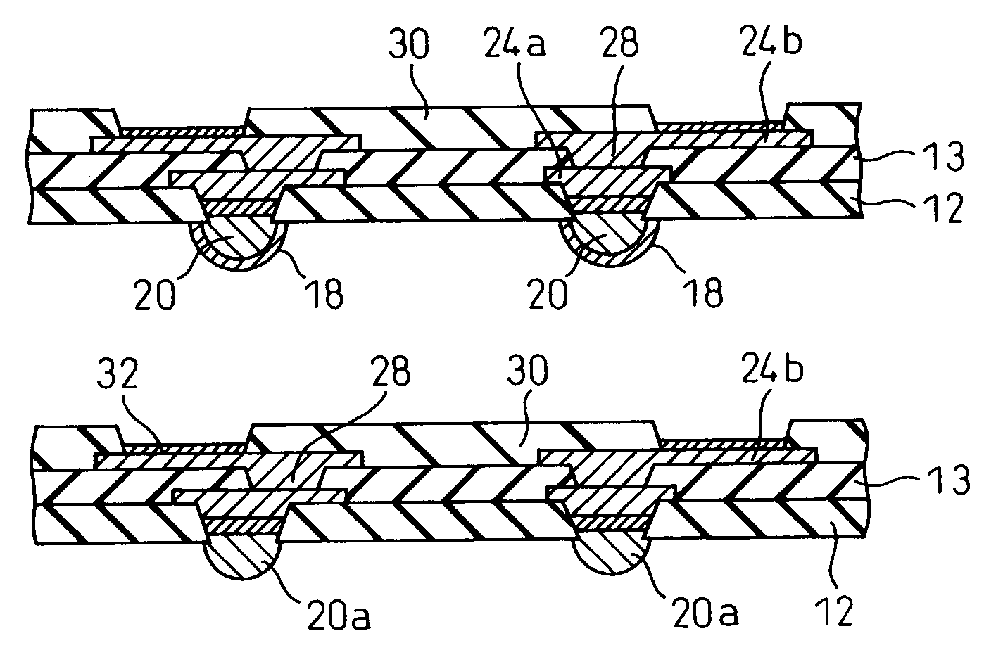
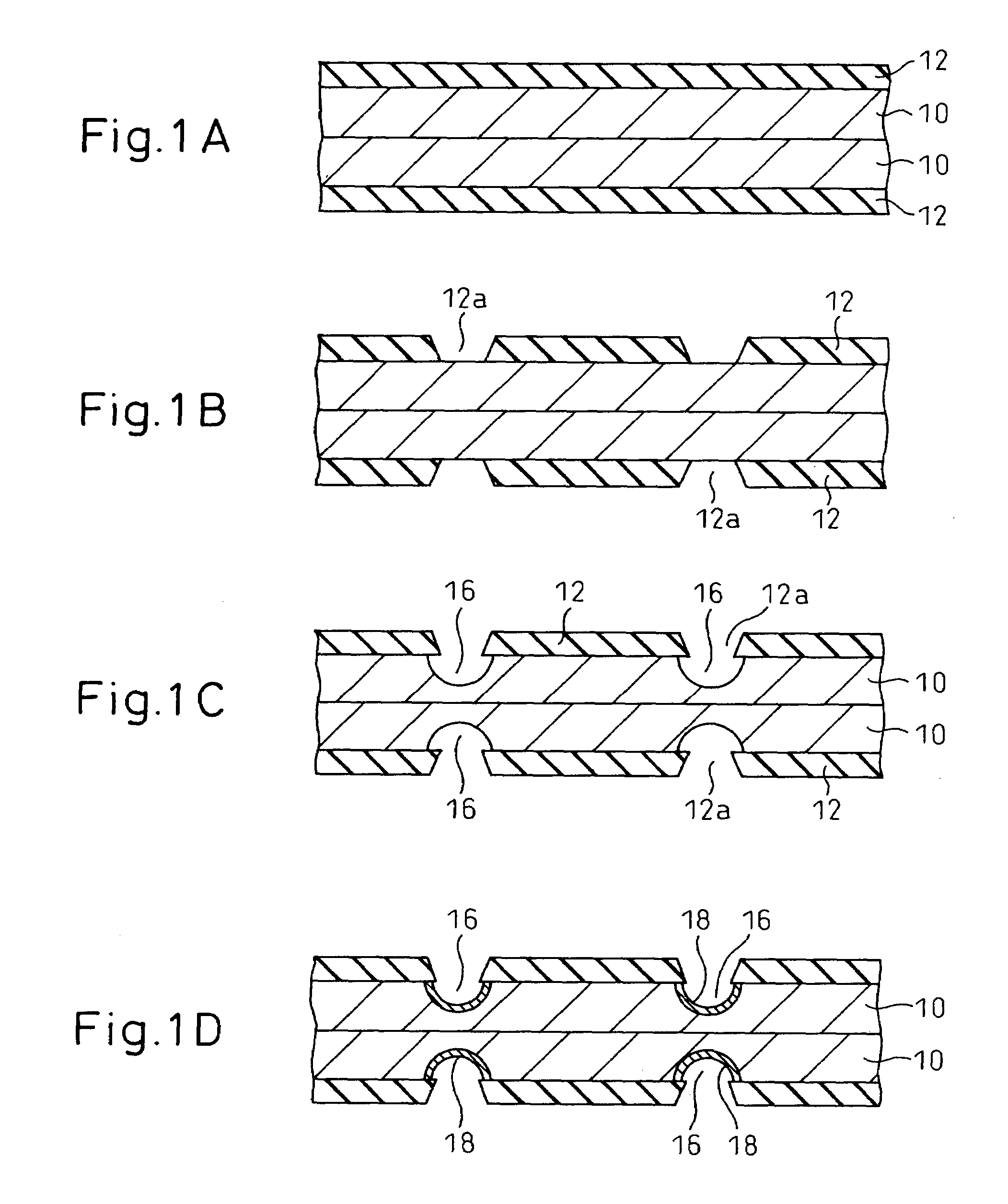
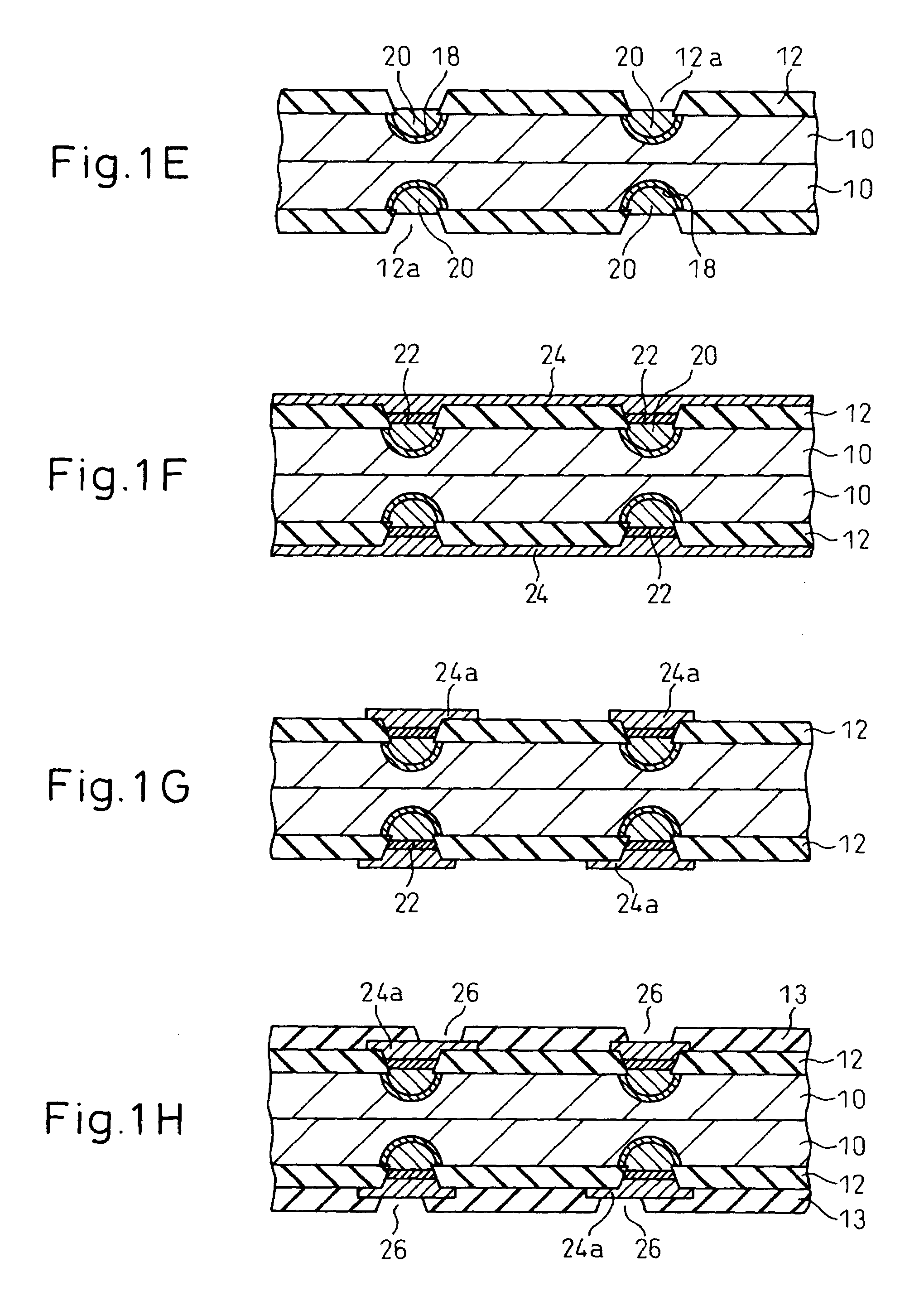
[0025]FIGS. 1A to 1M illustrate an embodiment of the invention, which represents the production of a wiring substrate provided with solder bumps on which a semiconductor element is to be mounted.

[0026]In this embodiment, a wiring substrate is produced by laminating two sheet-like bases made of a metal, forming solder bumps and wiring patterns on one side of each of the bases, dividing the laminated bases into two, and then dissolving each base for removal. The manufacturing process of the wiring substrate will now be described.

[0027]As shown in FIG. 1A, the opposed sides of the laminate of two bases 10, which form a core, are respectively covered with an insulating layer 12 exhibiting electrically insulating properties. The insulating layer 12 may be formed by laminating a electrically insulative resin film, such as a film of polyimide, to the base 10.

[0028]In this embodiment, a large-sized copper foil is used as the base 10, and a laminate of two large-sized bases 10 is used as a s...


PUM

PropertyMeasurementUnit
Diameteraaaaaaaaaa
Sizeaaaaaaaaaa
aaaaaaaaaa

Abstract

A wiring substrate with bumps protruding from a surface of the substrate covers one side of a metallic base with an electrical insulating film thereon, having open holes exposing the base, etching the base through the open holes to form concavities in the base, electroplating the interior faces of the concavities to form a barrier metal film thereon filling the concavities with a bump material by electroplating, and forming a barrler layer on the bump material in each concavity. A stack of wiring patterns is formed on the insulating film, adjacent wiring patterns being separated by a respective intervening insulating layer and being electrically connected to each other through vias in the intervening insulating layer, and to the bump material filled in the concavities. Thereafter, the base and barrier metal film are removed.

Description

BACKGROUND OF THE INVENTION[0001]1. Field of the Invention[0002]The invention relates to a method for producing a wiring substrate. More particularly, the invention relates to a method for producing a wiring substrate provided with connecting bumps and wiring patterns by the use of a base made of a metal.[0003]2. Description of the Related Art[0004]As a method of producing a wiring substrate, there is a method in which bumps to be subsequently connected to electrodes of a semiconductor element and a wiring pattern connected to the bumps are formed on one side of a base made of a metal, typically copper, and the base is then dissolved for removal, to thereby produce a wiring substrate, as described in JP 2000-323613 A and JP 2002-83893 A.[0005]For the formation of the wiring pattern on a base, a common method for producing a wiring substrate can be applied. For example, a method for forming a wiring layer having a given pattern by forming an insulating layer on a base, forming via ho...

Claims


Application Information

Patent Timeline
IPC IPC(8): B05D5/12C25D5/02H01L21/461H01L21/4763H05K3/20H05K3/34H05K3/36H05K3/46H01L21/48H01L21/68H01L23/498H05K3/40
CPCH01L21/4857H01L23/49816H05K3/3473H05K3/4007H01L21/6835Y10T29/49156H01L2221/68345H05K3/205H05K3/4644H05K2201/0367H05K2203/0338H05K2203/0376H05K2203/0384H05K2203/0726H01L2224/16225H01L2924/15311Y10T29/49165Y10T29/49144Y10T29/49126Y10T29/49128H01L2224/05573H01L2224/05568H01L2924/00014H01L2224/05599H05K3/46
Inventor IMAFUJI, KEIKODAIRA, TADASHICHINO, TAKESHINAKAMURA, JYUNICHIABE, MIWA
Owner SHINKO ELECTRIC IND CO LTD
Why Eureka
Try Eureka