TEM sample equipped with an identifying function, focused ion beam device for processing TEM sample, and transmission electron microscope

Active Publication Date: 2006-08-22
HITACHI HIGH TECH SCI CORP
View PDF4 Cites 26 Cited by
  • Summary
  • Abstract
  • Description
  • Claims
  • Application Information

AI Technical Summary

Problems solved by technology

As the observation surface is damaged by the digging processing, finishing processing is carried out while suppressing beam current and the surface is polished.
The completed sample is what the cut sample with sides in the order of 10 μm is fixed to a mesh base of diameter of approximately 3 mm, and this handling management is troublesome due to the sample being extremely small in size.
Even when it is said that the TEM sample is handled, after implemen

Method used


Image

  • TEM sample equipped with an identifying function, focused ion beam device for processing TEM sample, and transmission electron microscope
  • TEM sample equipped with an identifying function, focused ion beam device for processing TEM sample, and transmission electron microscope
  • TEM sample equipped with an identifying function, focused ion beam device for processing TEM sample, and transmission electron microscope

Examples


Embodiment Construction

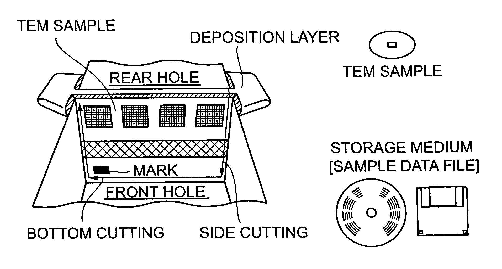
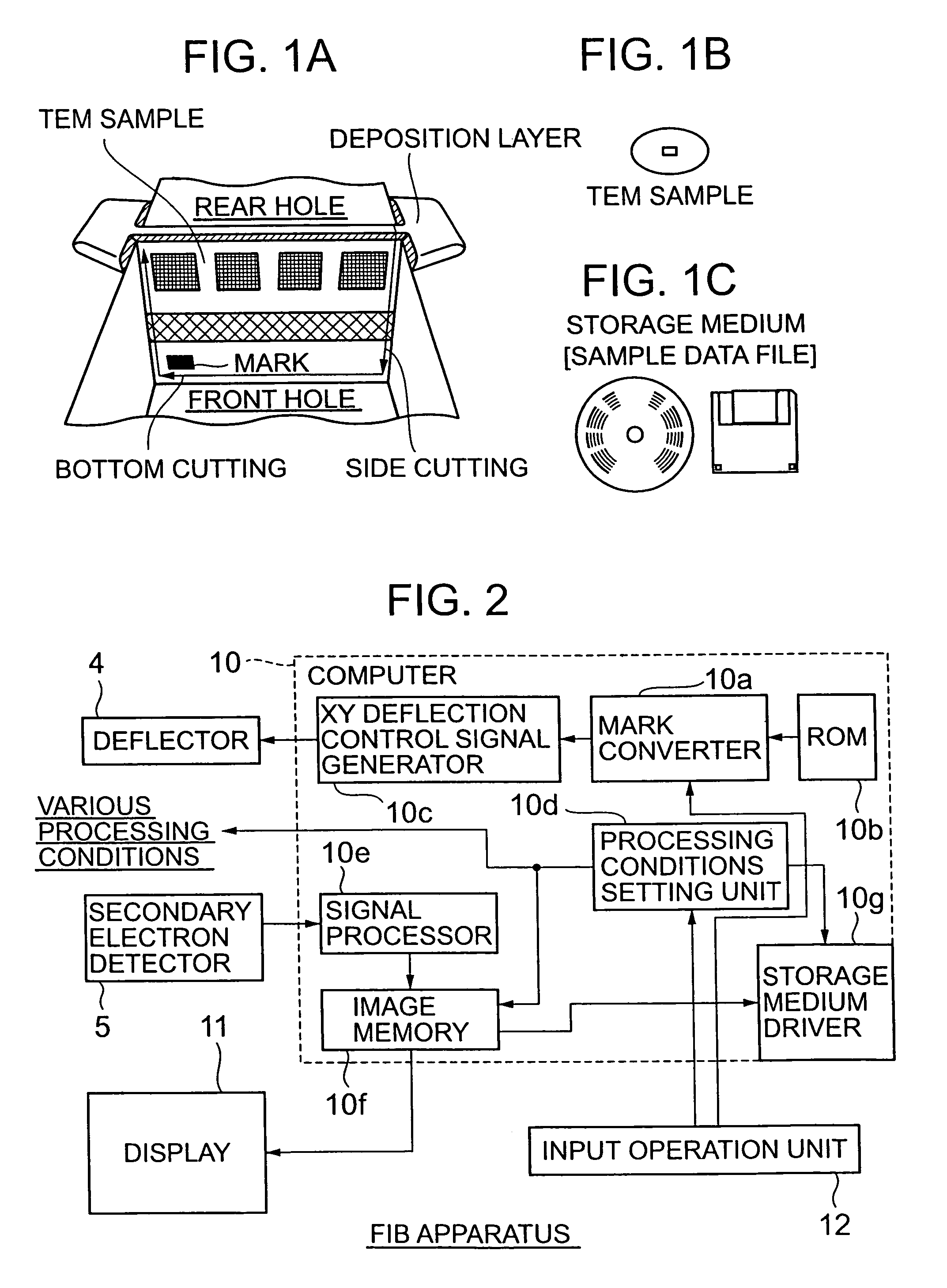
[0015]The present invention simplifies and enables straightforward execution of management of handling of TEM samples that are troublesome due to their minute size, and writes sample adjustment information using markings to the TEM sample itself. Means for inputting information specifying the sample and information associated with the sample, means for converting the information into an encoded marking, and means for making a signal for controlling an irradiation position of an FIB in order to process the mark at the sample surface and apply the signal to deflecting means are provided at the focused ion beam device making the TEM sample. Information specifying the TEM sample or related information associated with the sample is then written in a step of thin-processing the TEM sample body. The writing position is taken to be a position at the periphery of the sample so as not to be an observation target for the sample as shown in FIG. 1A, with it being beneficial to decide upon the w...


PUM


Abstract

The problem of the present invention is to provide a TEM sample equipped with an identifying function for easily specifying a detailed TEM sample and to provide a system for handling the management of information relating to the TEM sample using the TEM when making observations that is constructed with the FIB device manufacturing the sample. The TEM sample of the present invention is written with a mark encoding information specifying the sample at a specified location of a peripheral part. Information relating to the sample filed taking sample specifying information as an index is supplied to a TEM as associated matter. The sample working FIB device and observation TEM device of the present invention are provided with a function enabling writing of information relating to the sample and images to the file during operation which is then read out and utilized on a display.

Description

BACKGROUND OF THE INVENTION[0001]1. Field of the Invention[0002]The present invention relates to a transmission electron microscope (hereinafter referred to as TEM) sample marked with self-identifying information in a coded manner, and a TEM sample management system constructed between a focused ion beam (hereinafter referred to as FIB) device for producing the sample and a TEM for observing the sample.[0003]2. Description of the Related Art[0004]Making of semiconductor sliced samples for TEM observation by thin-processing using an FIB device is well-known. A method where a small part is cut-out mechanically from a wafer-shaped sample and this is processed to be thin and a method where etching processing is carried out on a wafer as is so as to extract a thin sample are well-known. The present invention relates to TEM samples made using the latter method. This TEM sample manufacturing method is as follows. First, a protective deposition film is formed by irradiating a processing por...

Claims


Application Information

Patent Timeline
IPC IPC(8): H01J37/26H01J37/304G01N1/32B01L3/00G01N1/28G01N35/00H01J37/24H01J37/305H01J37/317
CPCB01L3/545H01J37/304H01J37/3056B01L2300/021B01L2300/0822H01J2237/30416G01N2035/00772G01N1/32
Inventor ADACHI, TATSUYAFUJII, TOSHIAKIIWATSUKI, MASASHINARUSE, MIKIOSHEARER, MIKE HASSEL
Owner HITACHI HIGH TECH SCI CORP
Why Eureka
Try Eureka