Method for preparing observation sample of transmission electron microscope

An electron microscope and sample preparation technology, applied in the preparation of test samples, measuring devices, instruments, etc., can solve problems such as high cost, insufficient adhesion, and sample 3 falling, and achieve cost-saving effects

Inactive Publication Date: 2011-11-09
SEMICON MFG INT (SHANGHAI) CORP +1
View PDF5 Cites 12 Cited by
  • Summary
  • Abstract
  • Description
  • Claims
  • Application Information

AI Technical Summary

Problems solved by technology

[0004] When using the above-mentioned prior art to prepare the observation sample of the transmission electron microscope, when the sample 3 is adsorbed and placed on the sample observation grid 5 by using the glass rod 4, the risk of the sample 3 falling from the glass rod 4 is very high, and it must be determined by the technology. Only skilled personnel can complete the operation
At the same time, after the sample 3 is placed on the sample observation grid 5, there is still the problem that the sample 3 falls from the sample observation grid 5 when observed by a transmission electron microscope.
When the sample 3 together with the sample observation grid 5 is placed on the sample rod of the transmission electron microscope, it is often necessary to rotate the sample 3 together with the sample observation grid 5 at a certain angle for observation, and during this rotation process, due to The adhesion of the sample observation grid 5 is insufficient, and the sample 3 sometimes still falls from the sample observation grid. At this time, when observing through the transmission electron microscope, it will be found that the observation sample cannot be found, so the observers have to prepare the observation sample again
Therefore, the existing observation sample preparation method for transmission electron microscopy takes a long time, has low success rate and efficiency, and is expensive.

Method used


Image

  • Method for preparing observation sample of transmission electron microscope
  • Method for preparing observation sample of transmission electron microscope
  • Method for preparing observation sample of transmission electron microscope

Examples


Embodiment Construction

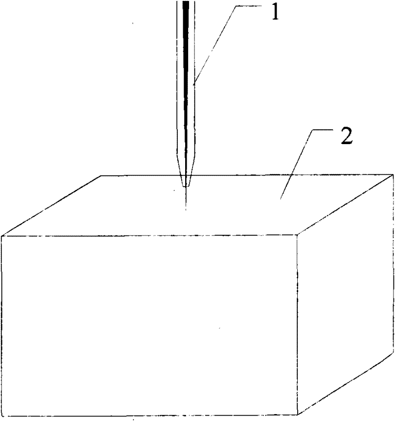
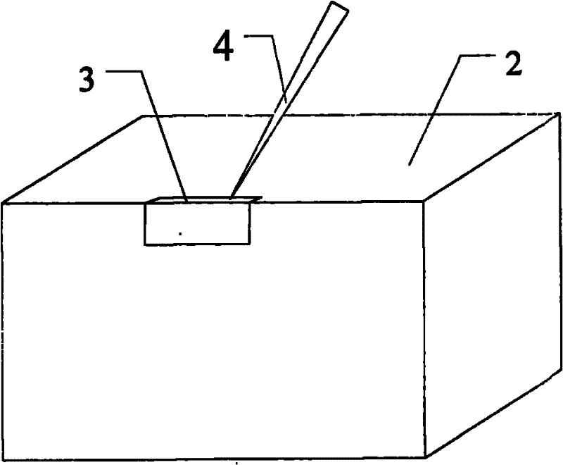
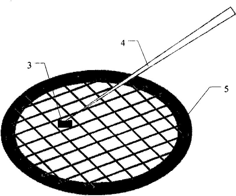
[0023] In order to make the above objects, features and advantages of the present invention more comprehensible, specific implementations of the present invention will be described in detail below in conjunction with the accompanying drawings.

[0024] A kind of transmission electron microscope observation sample preparation method described in the present invention can utilize multiple replacement modes to realize, and the following is to illustrate by preferred embodiment, certainly the present invention is not limited to this specific embodiment, and those in the art Common substitutions known to those of ordinary skill undoubtedly fall within the protection scope of the present invention.

[0025] Secondly, the present invention is described in detail using schematic diagrams. When describing the embodiments of the present invention in detail, for the convenience of illustration, the schematic diagrams are not partially enlarged according to the general scale, which should ...


PUM


Abstract

The invention provides a method for preparing an observation sample of a transmission electron microscope. The method comprises the following steps: selecting an electron microscope observation area on the surface of a pattern layer; removing a pattern layer and a substrate adjacent to one side of the electron microscope observation area to expose an image layer section and a substrate layer section on the side of the electron microscope observation area; removing a large part of the substrate of a semiconductor device, and maintaining a small part of the substrate; cutting the substrate in the electron microscope observation area to form a through groove; cutting the exposed pattern layer section on the side of the electron microscope observation area, which is adjacent to the through groove, so that different image layers on the pattern layer section have specific parts without other image layers or substrate in front of and behind the image layers and covering the image layers, wherein the specific parts of the image layers form a pattern layer observation area; and cutting the semiconductor device so that the size of the device containing the pattern layer observation area is in accordance with the size requirement to the sample of the transmission electron microscope.

Description

technical field [0001] The invention relates to the fields of semiconductor manufacturing technology and material analysis, in particular to a method for preparing a transmission electron microscope observation sample. Background technique [0002] Microstructures smaller than 0.2 μm cannot be seen clearly under an optical microscope, and these structures are called submicrostructures or ultrastructures. To see these structures clearly, it is necessary to choose a light source with a shorter wavelength to improve the resolution of the microscope. Since the wavelength of the electron beam is much shorter than that of visible light and ultraviolet light, a transmission electron microscope (TEM) uses the electron beam as the light source and uses the electromagnetic field as the lens to project the accelerated and concentrated electron beam onto a very thin sample. Above, electrons collide with atoms in the sample and change direction, resulting in solid angle scattering. The...

Claims


Application Information

Patent Timeline
Patent Type & Authority Applications(China)
IPC IPC(8): G01N1/28G01N13/00
Inventor 刘海君赖李龙张顺勇
Owner SEMICON MFG INT (SHANGHAI) CORP
Why Eureka
Try Eureka