
Electron holography method

a holography and electron technology, applied in the field of electron holography, can solve the problems of unsatisfactory ring spacing, and achieve the effect of improving resolution and sensitivity of electron holography

Active Publication Date: 2006-03-21
JEOL USA +1
View PDF11 Cites 13 Cited by
  • Summary
  • Abstract
  • Description
  • Claims
  • Application Information

AI Technical Summary

Benefits of technology

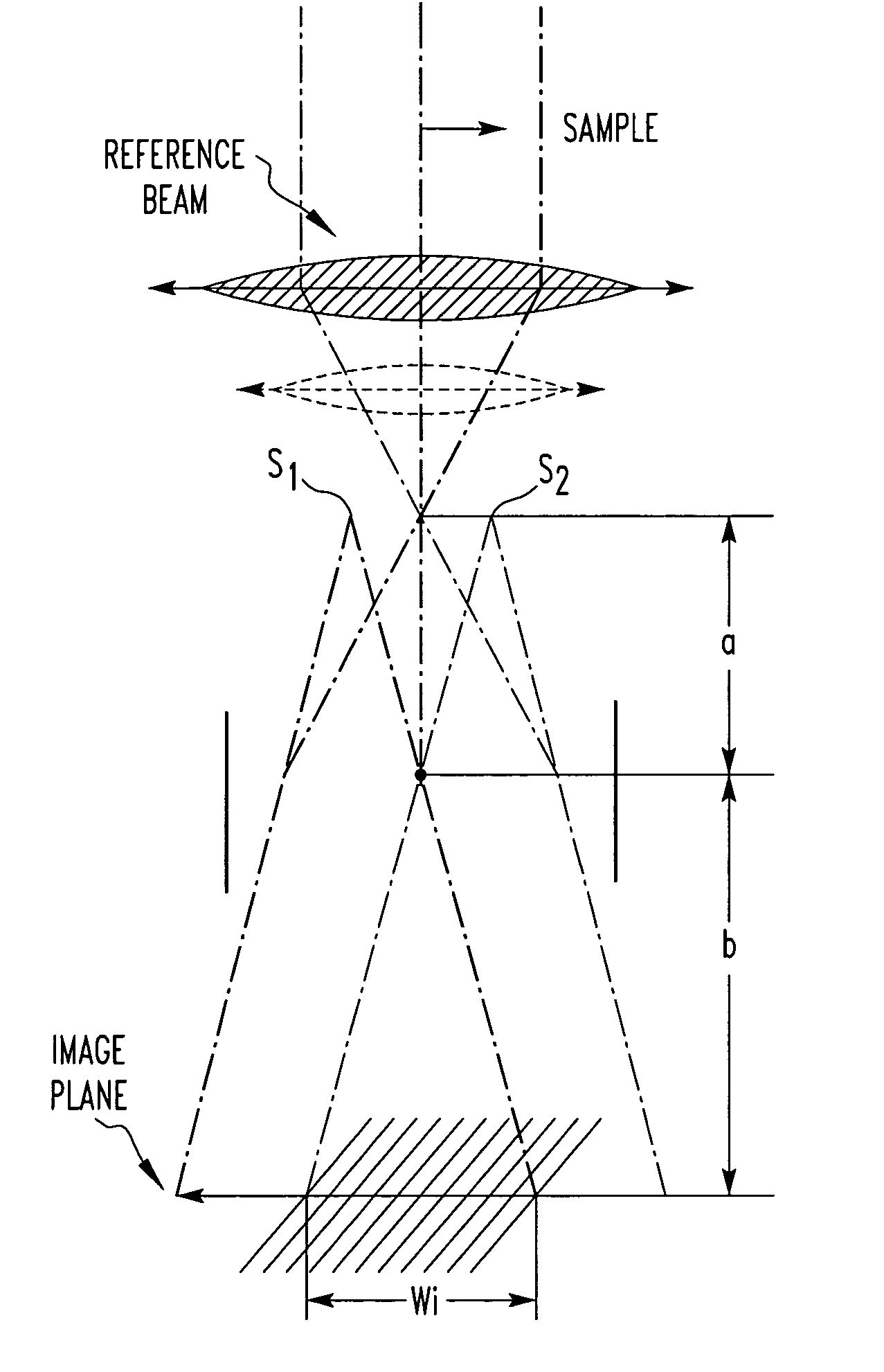
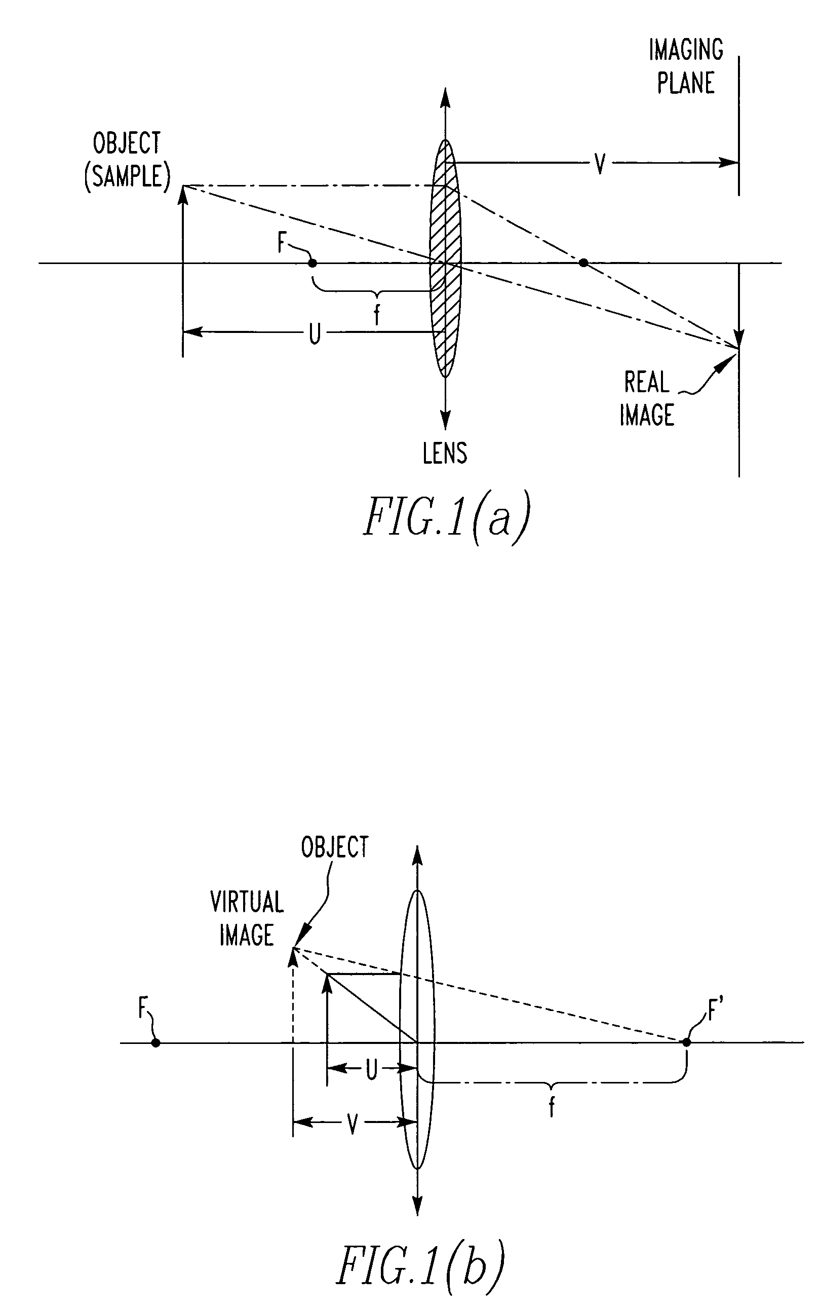
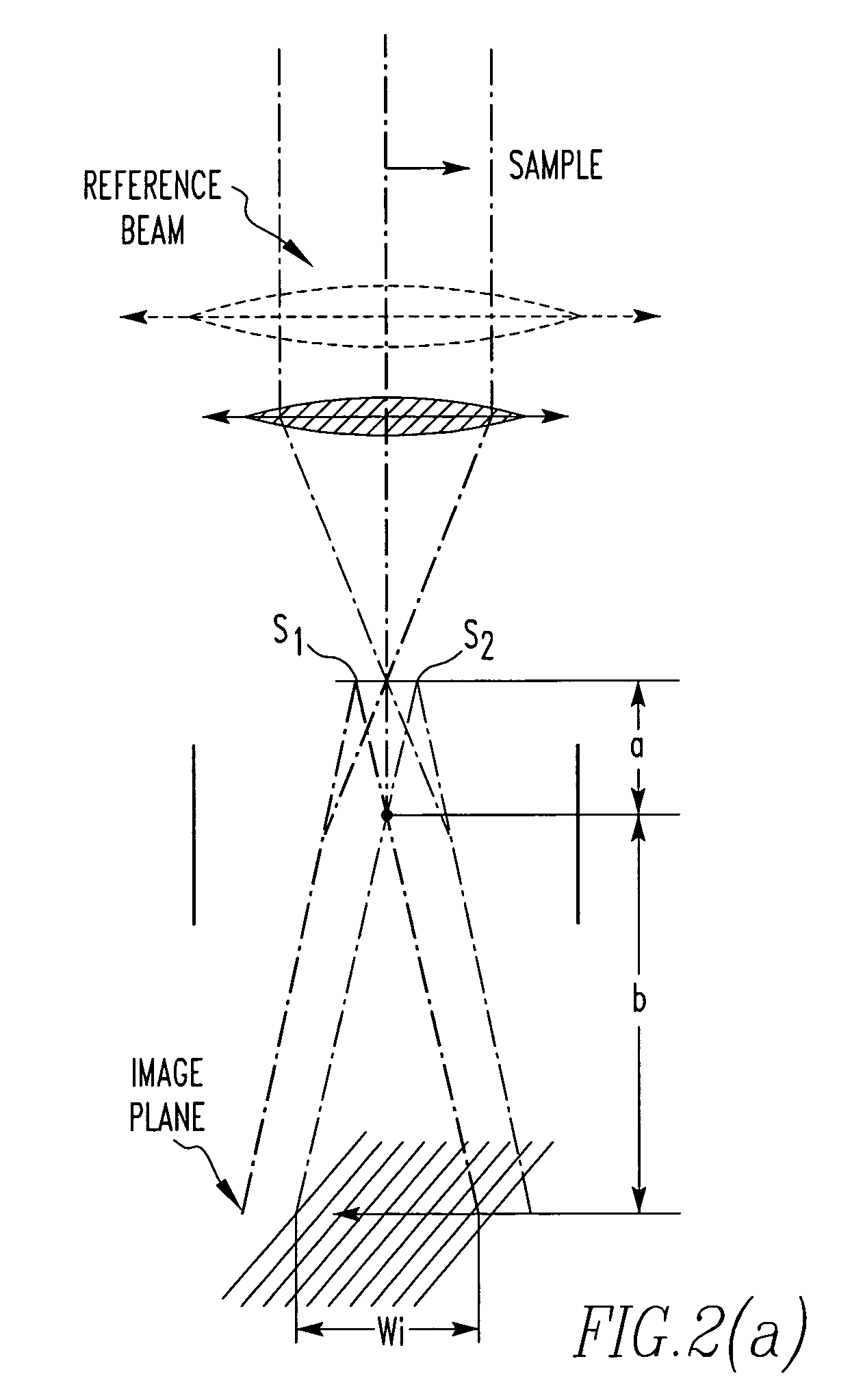
[0006]According to a preferred embodiment, the method comprises with the first objective lens forming a virtual image of a portion of the semiconductor device, with the second objective lens focussing the virtual image at an intermediate image plane beyond the biprism to form an intermediate image, adjusting the magnification of both of the objective lenses and the voltage applied the biprism to provide a field of view between 50 and 1,000 nanometers and a fringe spacing of between 1 and 10 nanometers with usable fringe contrast (5%–30%), and projecting the intermediate image onto the imaging means. The method allows fringe width and spacing relative to the object to be varied independently from the fringe contrast, resulting in enhanced resolution and sensitivity for electron holography.

Problems solved by technology

With some prior methods in which only one objective lens was used, if the overlap was satisfactory, the fringe spacing was unsatisfactory.

Method used


Image

  • Electron holography method
  • Electron holography method
  • Electron holography method

Examples


example

[0033]To demonstrate the flexibility of the dual lens method, we obtained electron holograms of pFET devices with poly silicon gate lengths of 220 nm and 70 nm on bulk Si and silicon on insulator (SOI) substrate, respectively. Samples were prepared by mechanically polished to a thickness of ˜400 nm and subsequently ion milled to a final thickness of ˜200–300 nm. To reduce the effects of charging, samples were coated on one side with ˜20 nm of carbon. The biprism voltage was held constant at ˜20V. Potential maps were reconstructed using the ASU plug-ins to Gatan Digital Micrograph. (see M. R. McCartney, Ultramicroscope 53, p. 283 (1994).

[0034]Contour potential maps for the two devices are shown in FIG. 7. Both devices exhibit symmetric doping profiles and the expected 1.0 V potential drop across the junctions. The intensity of the maps near the sides of the gates (side wall spacers and CoSi2) are wrapped over due to phase wrapping. As summarized in Table I, both σobj and Wobj can be ...


PUM


Abstract

An inline electron holograph method for observing a specimen with a transmission electron microscope having an electron gun, a collimating lens system, two spaced objective lenses, a biprism, and an imaging means comprises the steps of: with the first objective lens forming a virtual image of a portion of the specimen; with the second objective lens focussing the virtual image at an intermediate image plane to form an intermediate image; and projecting the intermediate image onto the imaging means.

Description

RELATED APPLICATION[0001]This application claims priority to provisional patent Application No. 60 / 438,968, filed Jan. 9, 2003 and incorporates that application by reference.BACKGROUND OF THE INVENTION[0002]Electron holography has become a desirable technique for inspection of semiconductor devices. The principles of electron holography are described, for example, in U.S. Published Patent Application 2002 / 0084412 entitled “Electron Microscope Equipped with Electron Biprism,” incorporated herein by reference, and U.S. Pat. No. 5,192,867 entitled “Electron Optical Measurement Apparatus”.[0003]The requirements for use of electron holography to inspect semiconductor devices are (1) an overlap of the plane wave transmitted through the specimen and the plane wave not transmitted through the specimen in the range of about 50 to 1000 nanometers, (2) fringe spacing between about 1 and 10 nanometers, and (3) adjustability of both the overlap and the fringe spacing. The overlap is roughly equi...

Claims


Application Information

Patent Timeline
IPC IPC(8): G03H5/00G21K7/00H01J37/26
CPCH01J37/26H01J2237/2614H01J2237/1514
Inventor WANG, YUN-YUKAWASAKI, MASAHIROBRULEY, JOHNDOMENICUCCI, ANTHONY G.GRIBELYUK, MICHAEL A.GAUDIELLO, JOHN G.
Owner JEOL USA
Learn More