
Multi-state magnetoresistance random access cell with improved memory storage density

a random access cell and magnetoresistance technology, applied in semiconductor devices, digital storage, instruments, etc., can solve the problem that the free magnetic moment vector will not be stable in either of these directions

Inactive Publication Date: 2006-08-22
EVERSPIN TECHNOLOGIES
View PDF11 Cites 58 Cited by
  • Summary
  • Abstract
  • Description
  • Claims
  • Application Information

AI Technical Summary

Benefits of technology

The patent describes a multi-state MRAM cell that includes a resistance device with a pinned anti-ferromagnetic region and a free ferromagnetic region. The free ferromagnetic region has a tri-layer structure with two easy axes and a first hard axis. The shape of the free ferromagnetic region creates multiple stable states that can be measured by measuring the resistance of the MRAM device. The technical effect of this patent is to provide a more efficient and reliable MRAM device with improved data storage capacity and stability.

Problems solved by technology

Consequently, the free magnetic moment vector will not be stable in either of these two directions.

Method used


Image

  • Multi-state magnetoresistance random access cell with improved memory storage density
  • Multi-state magnetoresistance random access cell with improved memory storage density
  • Multi-state magnetoresistance random access cell with improved memory storage density

Examples


Embodiment Construction

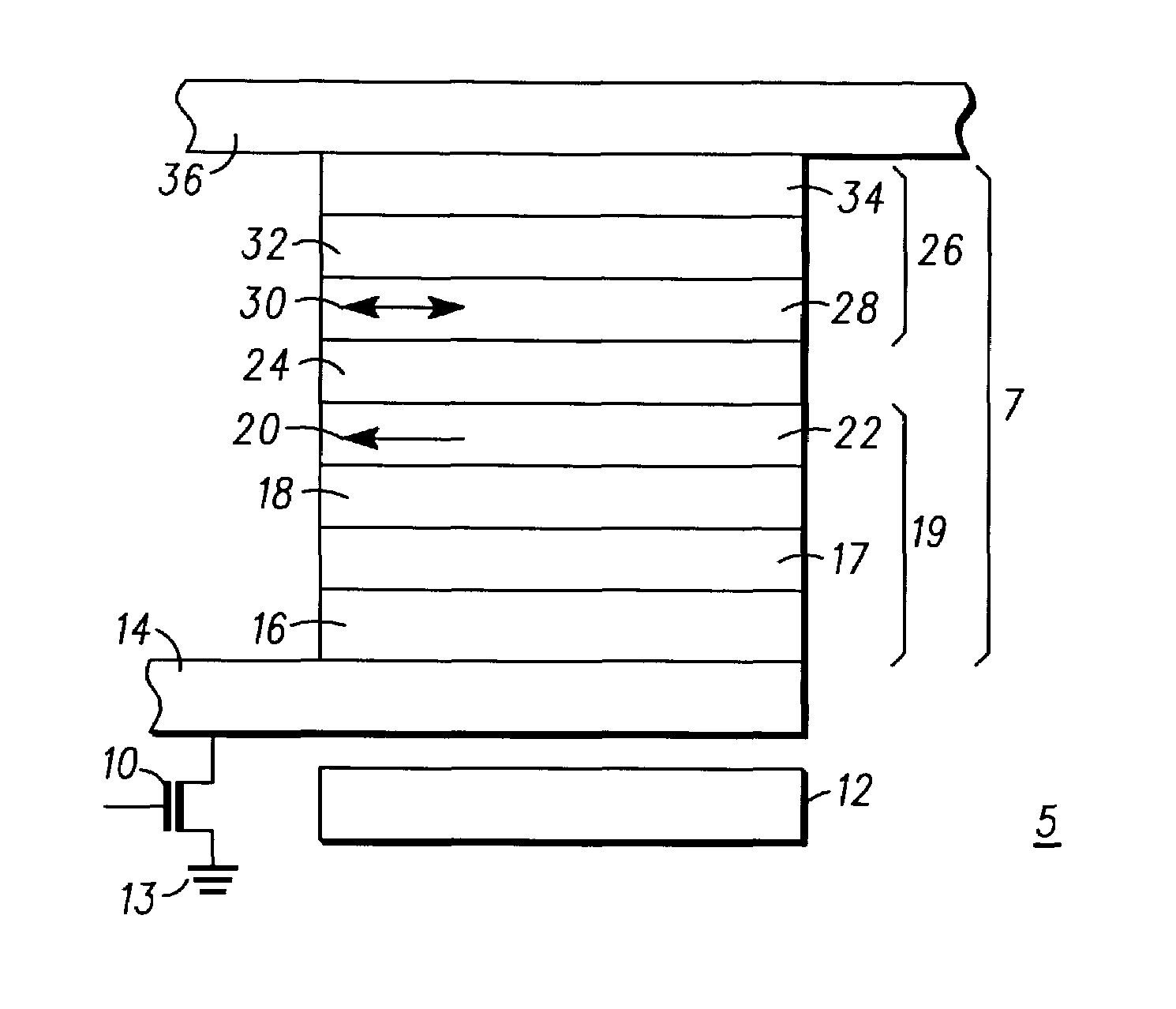
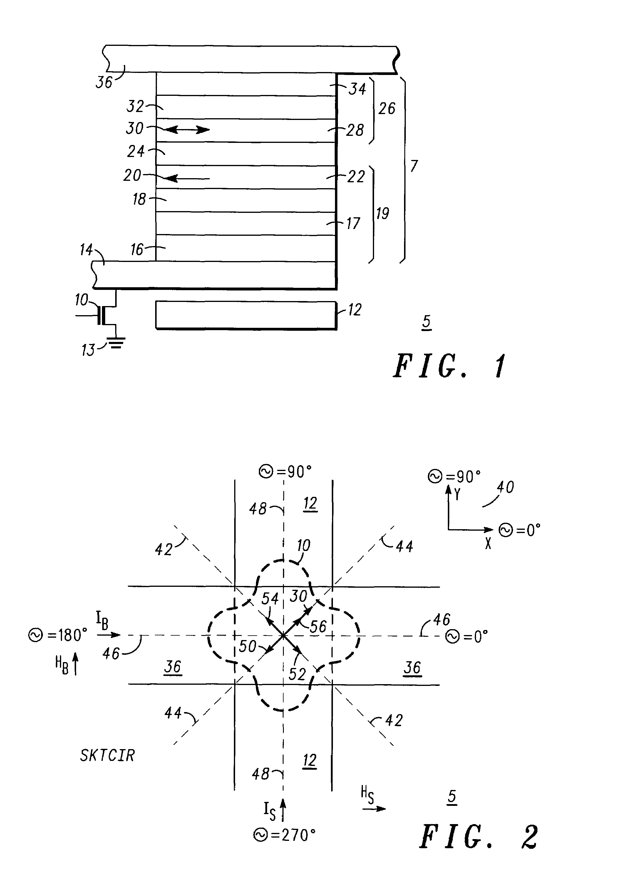
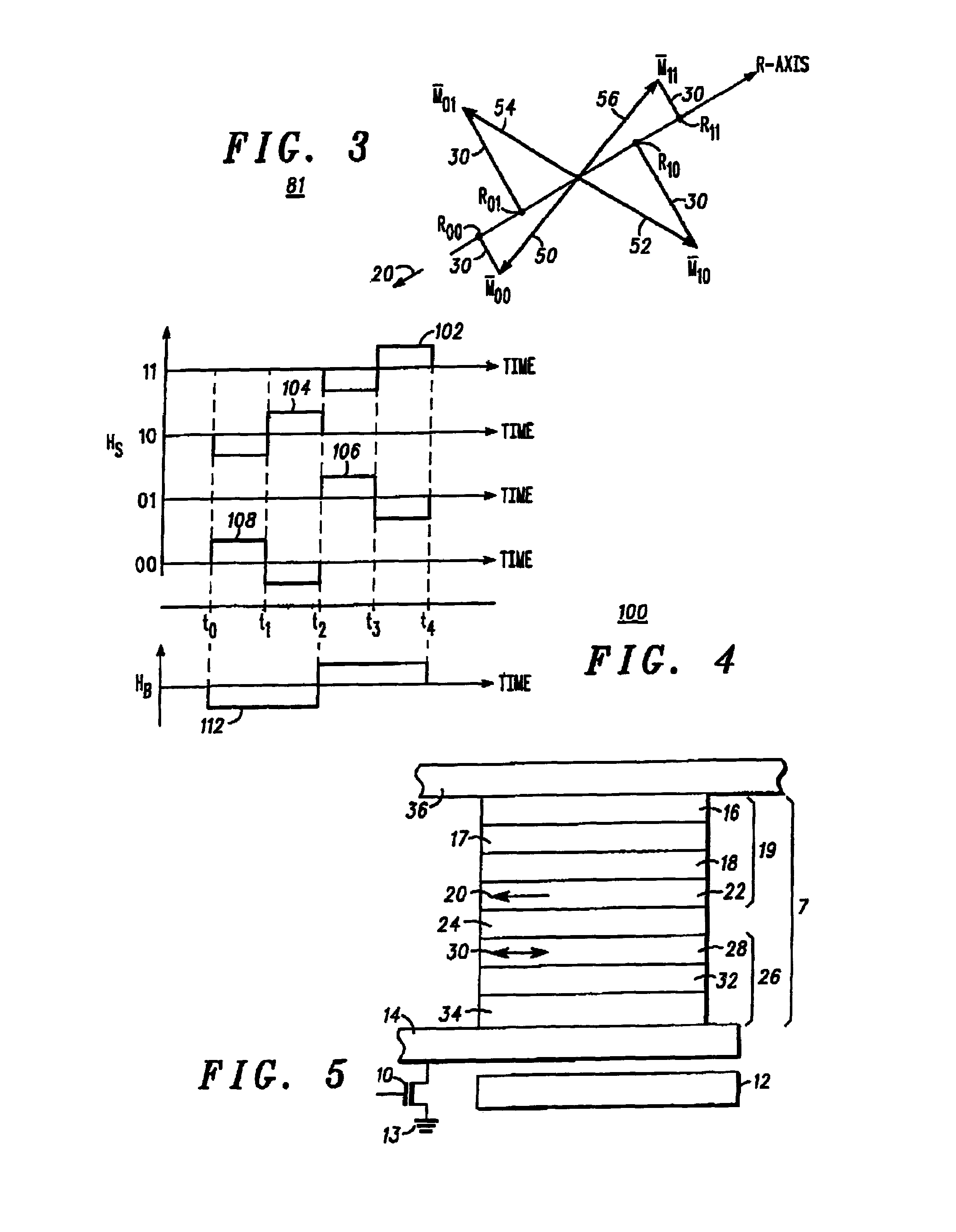
[0019]Turn now to FIG. 1, which illustrates a simplified sectional view of a multi-state MRAM cell 5 in accordance with the present invention. Multi-state MRAM cell 5 includes a multi-state MRAM device 7 sandwiched therebetween a base electrode 14 and a conductive line 36 wherein multi-state MRAM device 7 has a resistance, R. Further, a conductive line 12 is positioned proximate to base electrode 14 and an isolation transistor 10 is electrically connected to base electrode 14 and an electrical ground 13 as illustrated.

[0020]Multi-state MRAM device 7 includes a pinned synthetic anti-ferromagnetic region 19 positioned adjacent to base electrode 14. Pinned synthetic anti-ferromagnetic region 19 includes an anti-ferromagnetic pinning layer 16 positioned on base electrode 14, a pinned ferromagnetic layer 17 positioned on layer 16, an anti-ferromagnetic coupling layer 18 positioned on layer 17, and a fixed ferromagnetic layer 22 positioned on layer 18. Further, fixed ferromagnetic layer 2...


PUM


Abstract

A multi-state magnetoresistive random access memory device having a pinned ferromagnetic region with a magnetic moment vector fixed in a preferred direction in the absence of an applied magnetic field, an non-ferromagnetic spacer layer positioned on the pinned ferromagnetic region, and a free ferromagnetic region with an anisotropy designed to provide a free magnetic moment vector within the free ferromagnetic region with N stable positions, wherein N is a whole number greater than two, positioned on the non-ferromagnetic spacer layer. The number N of stable positions can he induced by a shape anisotropy of the free ferromagnetic region wherein each N stable position has a unique resistance value.

Description

[0001]This invention was made with Government support under Agreement No. MDA972-96 -3-0016 awarded by DARPA. The Government has certain rights in the invention.FIELD OF THE INVENTION[0002]This invention relates to semiconductor memory devices and, more particularly, the present invention relates to semiconductor random access memory devices that utilize a magnetic field.BACKGROUND OF THE INVENTION[0003]Traditional semiconductor memory devices store a memory state by storing an electronic charge. However, magnetoresistive random access memory (hereinafter referred to as “MRAM”) devices store a memory state by utilizing the direction of the magnetic moment vector created in a magnetic material or structure. Thus, a memory state in a MRAM device is not maintained by power, but rather by the direction of the magnetic moment vector. To be commercially viable, however, MRAM must have comparable memory density to current memory technologies, be scalable for future generations, operate at ...

Claims


Application Information

Patent Timeline
Patent Type & Authority Patents(United States)
IPC IPC(8): G11C11/00G11C11/15G11C11/56H01L21/8246H01L27/10H01L27/105H01L27/115H01L43/08
CPCG11C11/5607G11C11/16H10B61/00
Inventor SLAUGHTER, JON M.KORKIN, LEGAL REPRESENTATIVE, ANATOLI A.GORONKIN, HERBERTSAVTCHENKO, DECEASED, LEONID
Owner EVERSPIN TECHNOLOGIES
Learn More