
Re-configurable logic elements using heat assisted magnetic tunneling elements

a technology of heat-assist magnetic tunneling and logic elements, which is applied in the field of reconfigurable logic elements using heat-assist magnetic tunneling elements, can solve the problem that transistor-based logic cells cannot be reconfigured to perform alternate operations

Active Publication Date: 2006-08-29
SAMSUNG SEMICON
View PDF4 Cites 187 Cited by
  • Summary
  • Abstract
  • Description
  • Claims
  • Application Information

AI Technical Summary

Benefits of technology

Enables reconfigurable logic with a simpler structure, improving density and manufacturing ease by using a single magnetic element per cell and allowing for various logic operations like AND, OR, NAND, and NOR without complex interconnections.

Problems solved by technology

Thus, the transistor based logic cells cannot be reconfigured to perform alternate operations.

Method used


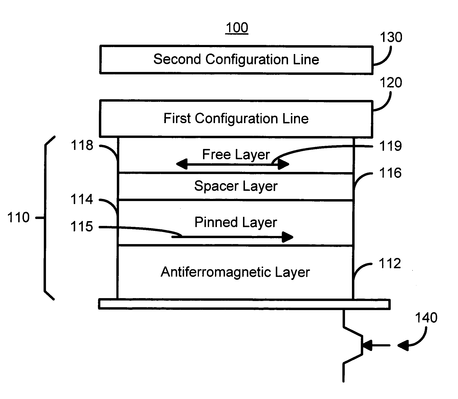
Image

  • Re-configurable logic elements using heat assisted magnetic tunneling elements
  • Re-configurable logic elements using heat assisted magnetic tunneling elements
  • Re-configurable logic elements using heat assisted magnetic tunneling elements

Examples


Embodiment Construction

[0018]The present invention relates to logic design. The following description is presented to enable one of ordinary skill in the art to make and use the invention and is provided in the context of a patent application and its requirements. Various modifications to the preferred embodiments and the generic principles and features described herein will be readily apparent to those skilled in the art. Thus, the present invention is not intended to be limited to the embodiments shown, but is to be accorded the widest scope consistent with the principles and features described herein.

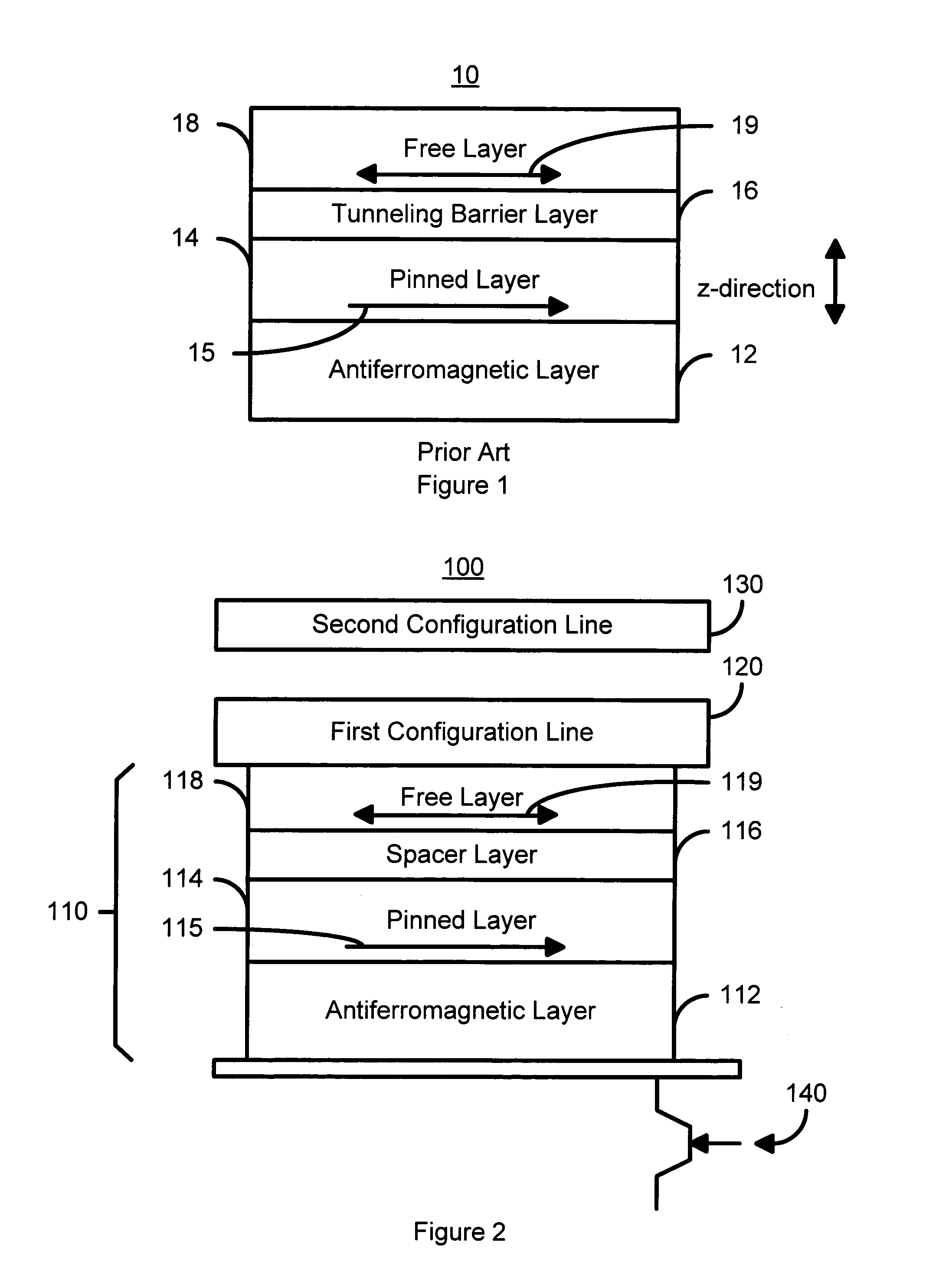
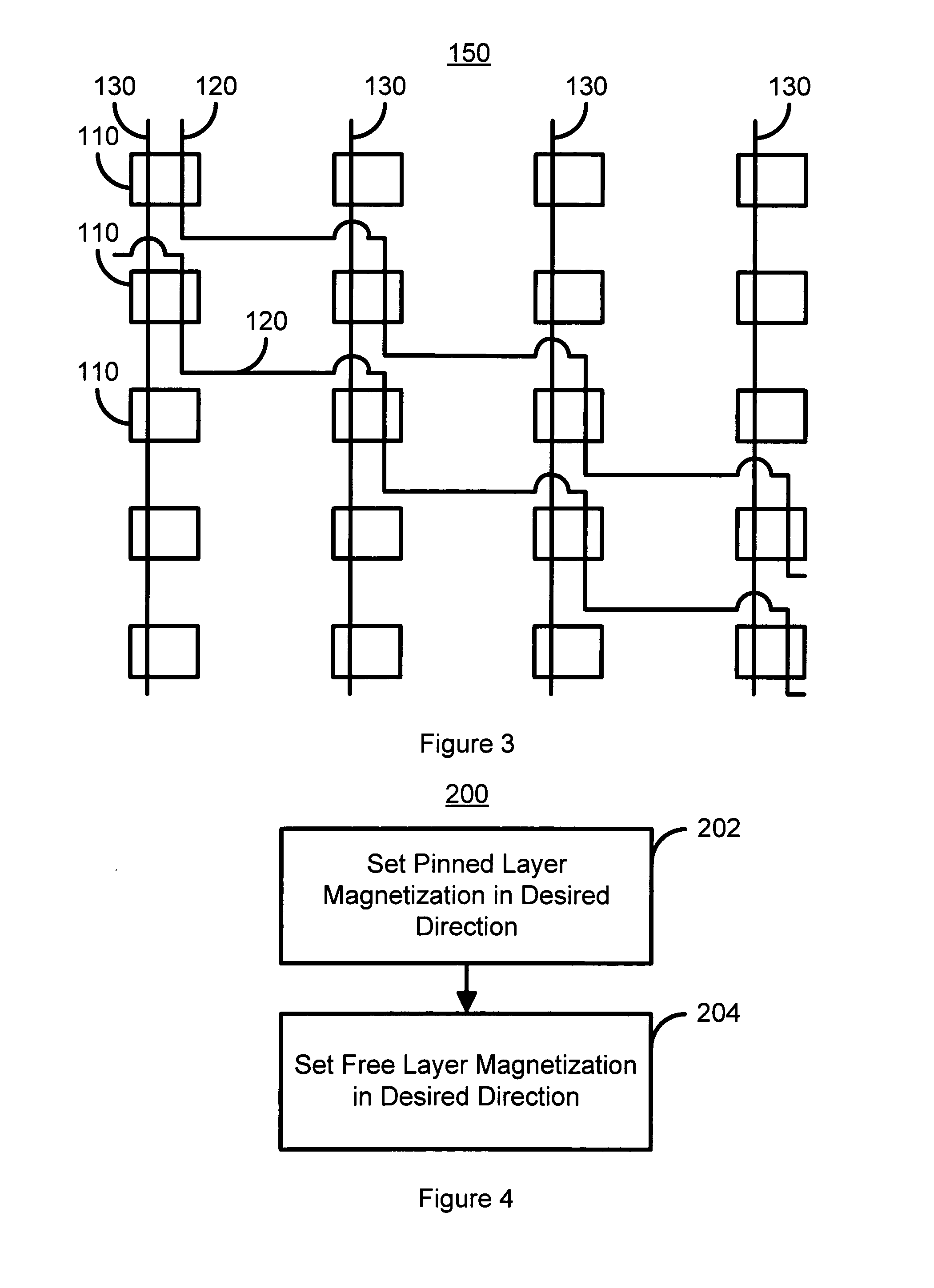
[0019]The present invention provides a magnetic logic cell that includes a magnetic element having a pinned layer, a free layer, and a spacer layer. The pinned layer has a pinned layer magnetization. The free layer has a free layer magnetization. The spacer layer resides between the pinned layer and the free layer. A first configuration line is electrically connected to the magnetic element and carries a f...


PUM

PropertyMeasurementUnit
blocking temperatureaaaaaaaaaa
thicknessaaaaaaaaaa
lengthaaaaaaaaaa

Abstract

A magnetic logic cell includes a magnetic element having a pinned layer, a free layer, and a spacer layer. The pinned and free layers have pinned and free layer magnetizations. The spacer layer resides between the pinned and free layers. In one aspect, the magnetic logic cell includes a first configuration line that is electrically connected to the magnetic element and carries a first current and a second configuration line electrically that is insulated from the magnetic element and the first configuration line and carries a second current. The first or second current alone cannot switch the free layer magnetization. The first and second currents together can switch the free layer magnetization. When the first current is driven through the magnetic element and the second current is provided, the combination sets the pinned layer magnetization direction. In one aspect, the pinned layer magnetization is set by heating the AFM layer to approximately at or above the blocking temperature. In order to configure the logic cell, an initial direction for the free layer magnetization is also set.

Description

FIELD OF THE INVENTION[0001]The present invention relates to electronic logic devices and more particularly to a method and system for providing a magnetic element that is suitable for use in logic applications such as AND, OR, NAND, and NOR gates.BACKGROUND OF THE INVENTION[0002]Currently, magnetic elements are of interest for a variety of applications. In general, such conventional magnetic elements are magnetic tunneling junctions. FIG. 1 depicts such a conventional magnetic element 10. The conventional magnetic element 10 includes a conventional antiferromagnetic (AFM) layer 12, a conventional pinned layer 14, a conventional tunneling barrier layer 16, and a conventional free layer 18. Other layers (not shown), seed, and / or capping layers may also be used. The conventional pinned layer 14 and the conventional free layer 18 are ferromagnetic. Thus, the conventional free layer 18 is depicted as having a changeable magnetization 19. The nonmagnetic tunneling barrier layer 16 is typ...

Claims


Application Information

Patent Timeline
Patent Type & Authority Patents(United States)
IPC IPC(8): H01L31/062H01F10/32H01L29/76H03K19/168H10N50/10
CPCB82Y25/00H03K19/168H01L43/08H01F10/3254H10N50/10
Inventor PAKALA, MAHENDRAHUAI, YIMING
Owner SAMSUNG SEMICON
Learn More