Technology mapping technique for fracturable logic elements

a technology of logic elements and technology mapping, applied in the field of electronic design automation of logic design, to achieve the effect of minimizing circuit area and small final circuit area

Inactive Publication Date: 2006-08-29
ALTERA CORP
View PDF25 Cites 20 Cited by
  • Summary
  • Abstract
  • Description
  • Claims
  • Application Information

AI Technical Summary

Benefits of technology

This patent describes a new way to make circuits faster and cheaper by using fracturable logic elements called "minimizers". These minis have two parts - they're either very big or really tiny. When making the map from scratch, the system tries to evenly distribute these minis among different functions in order to get the best results. It also keeps the number of maxi ones low because those tend to absorb too much space. Overall, this method makes it possible to create smaller, efficient circuits without sacrificing their functionality.

Problems solved by technology

The technical problem addressed in this patent is how to optimize the design of programmable logic circuits containing millions of logic elements. With advances in semiconductor technologies, these circuits offer increased complexity and opportunities for improvement through efficient use of fracturable logic elements. This requires effective design automation methods that make proper functioning and high performance possible while minimizing resource usage.

Method used


Image

  • Technology mapping technique for fracturable logic elements
  • Technology mapping technique for fracturable logic elements
  • Technology mapping technique for fracturable logic elements

Examples


Embodiment Construction

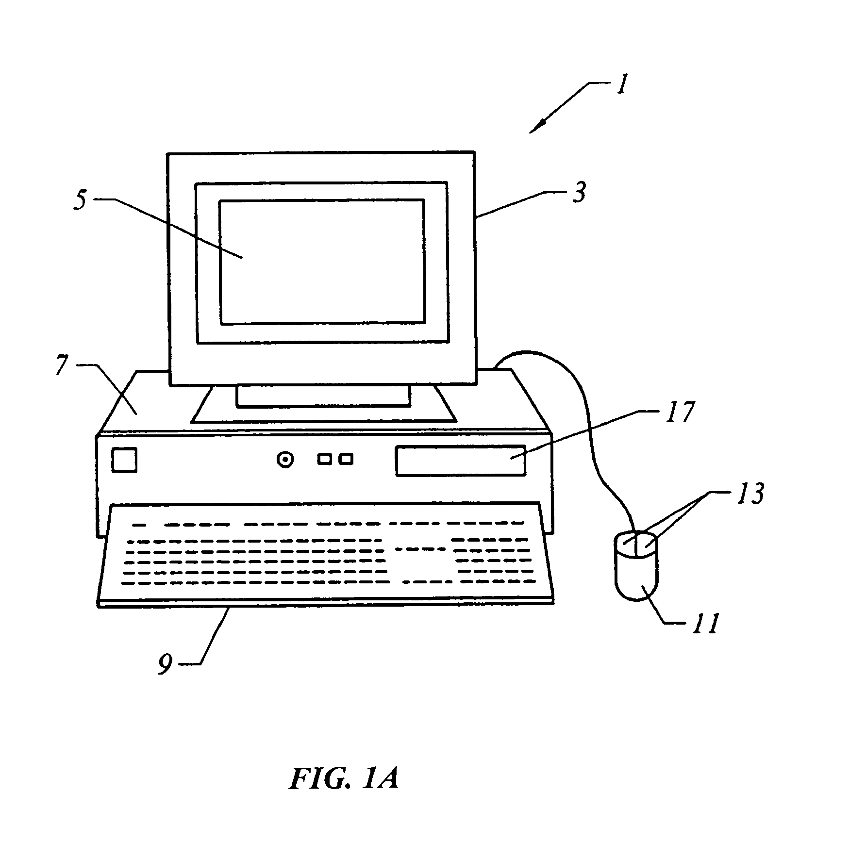
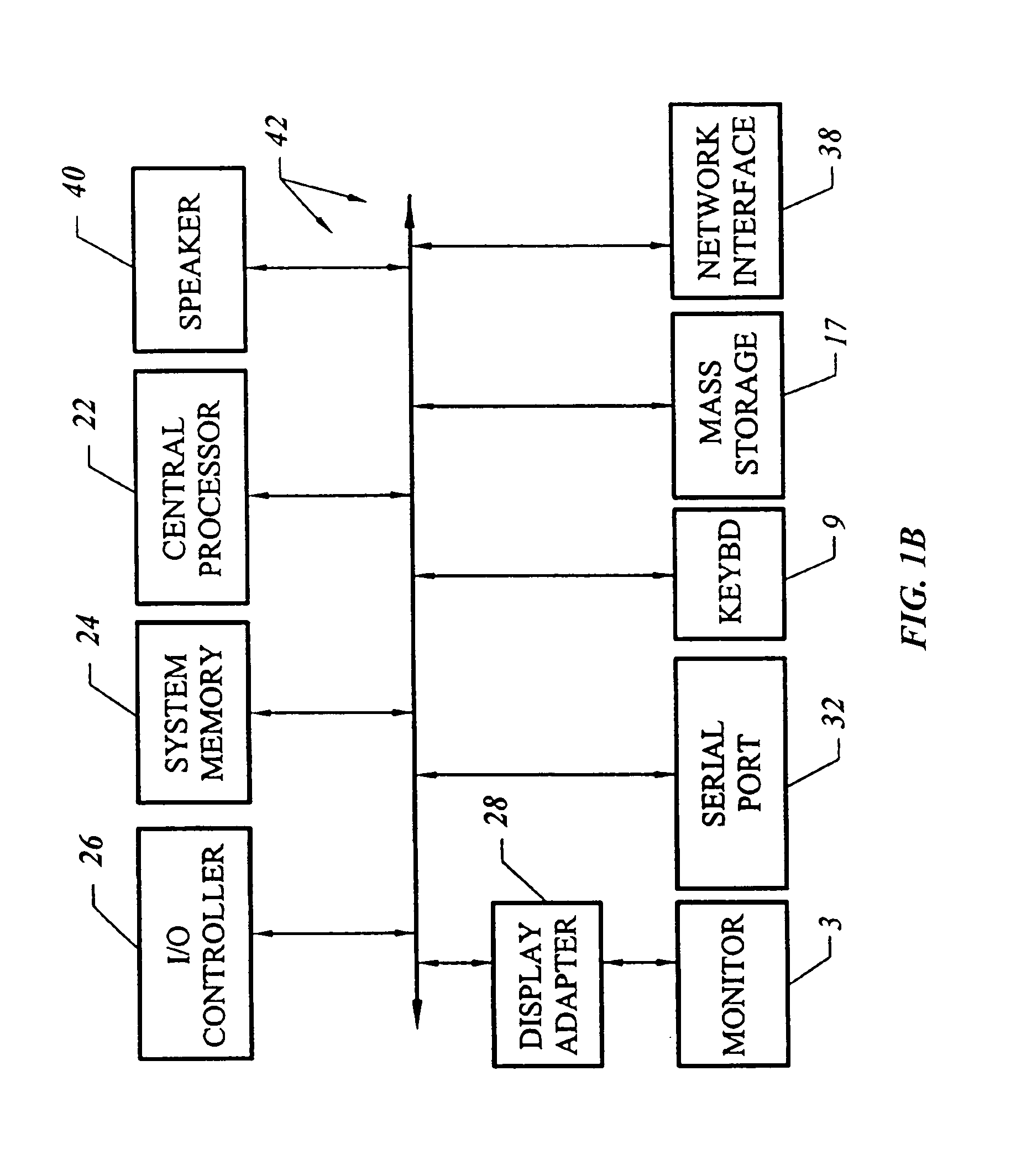
[0030]FIG. 1A shows a system of the present invention for performing synthesis and place and route. In an embodiment, software of the invention executes on a computer workstation system, such as shown in FIG. 1A. FIG. 1A shows a computer system 1 that includes a monitor 3, screen 5, cabinet 7, keyboard 9, and mouse 11. Mouse 11 may have one or more buttons such as mouse buttons 13. Cabinet 07 houses familiar computer components, some of which are not shown, such as a processor, memory, mass storage devices 17, and the like. Mass storage devices 17 may include mass disk drives, floppy disks, Iomega ZIP™ disks, magnetic disks, fixed disks, hard disks, CD-ROMs, recordable CDs, DVDs, DVD-R, DVD-RW, Flash and other nonvolatile solid-state storage, tape storage, reader, and other similar media, and combinations of these. A binary, machine-executable version, of the software of the present invention may be stored or reside on mass storage devices 17. Furthermore, the source code of the sof...


PUM


Abstract

A technique of minimizes circuit area on programmable logic with fracturable logic elements by using “balancing” in the technology mapping stage of the programmable logic computer-aided-design flow. A fracturable LE can be used for logic implementation in many ways, such as being used as one maximum-sized look-up table (LUT) or multiple smaller LUTs. One of more inputs of the multiple smaller LUTs may be shared. By balancing, this means mean that the technology mapping algorithm is tuned to use more small LUTs and fewer maximum-sized LUTs to implement the circuit. Although this is counterintuitive since the larger LUTs are more effective at absorbing gates, the technique achieves a smaller final circuit area by packing small LUTs into fracturable LEs.

Description


Claims


Application Information

Patent Timeline
Owner ALTERA CORP
Why Eureka
Try Eureka